Advanced PCB Design Techniques: Implementing via-in-pad for High-Density Applications
Advanced PCB Design Techniques: Implementing Via-in-Pad for High-Density Applications Introduction In the realm of high-density electronics, the demand for compact and efficient PCB designs is ever-gr...
Introduction
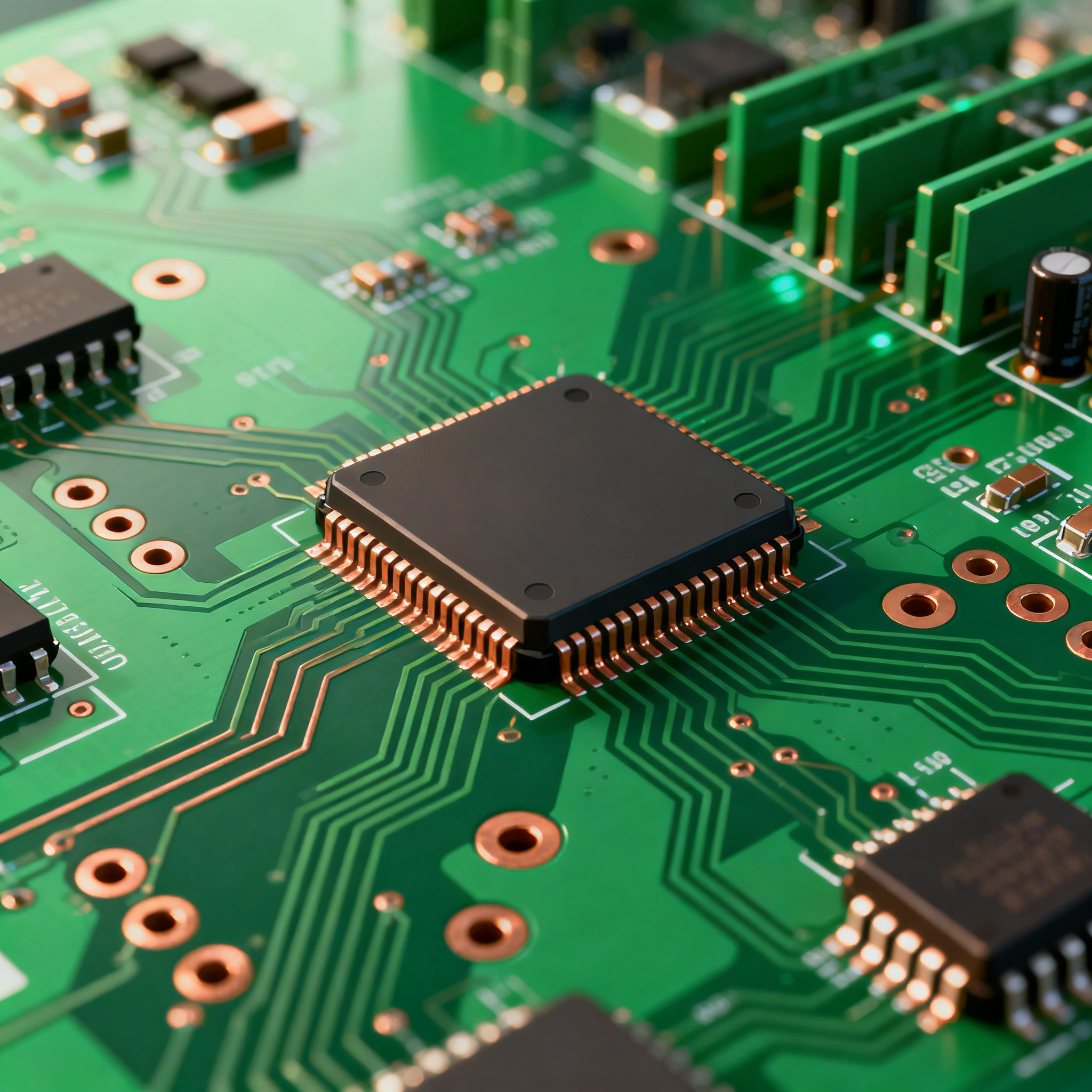
In the realm of high-density electronics, the demand for compact and efficient PCB designs is ever-growing. One of the advanced techniques to achieve this is via-in-pad, which allows for the integration of vias directly beneath the pads of components. This technique is invaluable in applications where space is a premium, such as in mobile devices, wearables, and advanced computing systems. Understanding the intricacies of implementing via-in-pad can significantly enhance the performance and reliability of electronic devices, making it an essential skill for modern PCB designers.
Technical Overview
Via-in-pad is a sophisticated PCB design method that involves placing vias directly under component pads. This technique is particularly useful in high-density interconnect (HDI) designs where space is limited. The primary advantage of via-in-pad is its ability to reduce the inductance and resistance of the electrical path, leading to improved signal integrity and thermal performance. This method also facilitates the routing of signals in multi-layer boards, which is crucial for complex designs. However, it requires careful consideration of manufacturing processes and materials to avoid issues such as solder wicking and voids.
Detailed Specifications
When selecting components for via-in-pad designs, several specifications are critical. These include CPU speed, memory capacity, peripheral interfaces, power requirements, and packaging options. Understanding these specifications helps in choosing the right components that align with the design goals and application requirements.
| Specification | Details | Importance |
|---|---|---|
| CPU Speed | 1.8 GHz | Determines processing power |
| Memory | 4 GB DDR4 | Influences multitasking capability |
| Peripherals | USB 3.0, HDMI | Connectivity options |
| Power Consumption | 5V, 2A | Impacts thermal design |
| Package Type | BGA | Affects assembly process |
| Operating Temperature | -40°C to 85°C | Environmental suitability |
| Storage | eMMC 64GB | Data retention and speed |
| Graphics | Integrated GPU | Visual performance |
| Networking | Wi-Fi 6, Bluetooth 5.0 | Wireless connectivity |
| Dimensions | 35mm x 35mm | Physical footprint |
Key Takeaways from the Specifications
The core specifications table provides a comprehensive overview of the essential attributes of a component suitable for via-in-pad designs. The CPU speed and memory specifications are crucial for ensuring that the PCB can handle the required processing loads efficiently. Peripherals and networking options highlight the component's connectivity capabilities, which are vital for integrated systems. Power consumption and operating temperature range are critical for ensuring reliability and performance under various conditions. Understanding these specifications helps in selecting components that meet the design requirements and application demands.
| Electrical Parameter | Value | Significance |
|---|---|---|
| Operating Voltage | 3.3V | Standard for digital circuits |
| Maximum Current | 500mA | Determines power handling |
| Input Impedance | 50 Ohms | Signal integrity |
| Output Impedance | 50 Ohms | Minimizes reflections |
| Signal Rise Time | 0.5 ns | Affects signal quality |
| Propagation Delay | 1.2 ns | Timing accuracy |
| ESD Protection | 2 kV | Prevents damage from static |
| Power Dissipation | 1.5W | Thermal management |
| Input Capacitance | 2 pF | Impacts high-frequency response |
| Output Capacitance | 3 pF | Influences signal drive strength |
Practical Implications
The electrical characteristics table provides insights into the operational parameters of the component. The operating voltage and current define the power requirements and compatibility with the power supply. Impedance values are crucial for maintaining signal integrity and minimizing losses. Timing parameters such as rise time and propagation delay are vital for ensuring accurate signal transmission, especially in high-speed applications. ESD protection and power dissipation values are important for safeguarding the component against electrical overstress and managing heat dissipation effectively.
| Application | Configuration | Benefits |
|---|---|---|
| Mobile Devices | Compact BGA | Space-saving design |
| Wearables | Low Power | Extended battery life |
| Automotive | Robust ESD | Enhanced reliability |
| IoT Devices | Wi-Fi/Bluetooth | Seamless connectivity |
| Medical Equipment | High Precision | Accurate data processing |
| Industrial Controls | High Temperature | Environmentally resilient |
| Consumer Electronics | Multimedia Support | Rich user experience |
Application Guidelines
The application comparison table highlights various use cases and configurations for components in via-in-pad designs. Each application has specific requirements, such as compact design for mobile devices or robust ESD protection for automotive applications. Understanding these configurations and their benefits helps in selecting the right components for specific applications, ensuring optimal performance and reliability. For instance, low power configurations are ideal for wearables to extend battery life, while high precision configurations are crucial for medical equipment to ensure accurate data processing.
Design Considerations
Implementing via-in-pad in PCB designs requires careful consideration of several factors to ensure successful integration and optimal performance. First, it's essential to collaborate closely with the PCB manufacturer to understand their capabilities and constraints, as via-in-pad involves complex manufacturing processes. The choice of materials is crucial, as different substrates and finishes can impact thermal performance and reliability. Additionally, designers must account for potential issues such as solder wicking, which can lead to poor solder joint formation and component failure.
Thermal management is another critical aspect, as via-in-pad can alter the thermal profile of the PCB. Proper heat dissipation techniques, such as thermal vias or heat sinks, may be necessary to prevent overheating. Signal integrity must also be addressed, as the placement of vias can affect impedance and cause reflections. Simulation tools can help optimize the layout and ensure signal integrity. Finally, thorough testing and validation are essential to identify and rectify any issues before mass production.
Step-by-Step Implementation
- Define the design requirements and constraints, including size, power, and connectivity needs.
- Select appropriate components that support via-in-pad, considering specifications such as package type and power consumption.
- Collaborate with the PCB manufacturer to understand their capabilities and design rules for via-in-pad.
- Design the PCB layout, placing vias directly under component pads to save space and improve routing.
- Use simulation tools to analyze signal integrity and thermal performance, making adjustments as needed.
- Create a prototype of the PCB design and conduct thorough testing to identify and resolve any issues.
- Finalize the design based on test results and prepare for mass production, ensuring all specifications are met.
- Work with the manufacturer to oversee the production process, ensuring quality and consistency.
Common Issues & Solutions
- Solder Wicking: Use solder mask over vias to prevent solder from flowing into the via during assembly.
- Voids in Solder Joints: Optimize reflow profiles to reduce void formation and ensure strong solder joints.
- Impedance Mismatch: Adjust trace widths and via placement to maintain consistent impedance throughout the PCB.
- Thermal Management: Implement thermal vias or heat sinks to dissipate heat effectively and prevent overheating.
- Signal Integrity: Use simulation tools to analyze and optimize signal paths, minimizing reflections and losses.
- Manufacturing Variability: Collaborate closely with the manufacturer to ensure consistent quality and address any process variations.
Applications & Use Cases
Via-in-pad is widely used in various applications that require compact and efficient designs. In mobile devices, it enables space-saving layouts, allowing for more features in smaller form factors. Wearable technology benefits from low power configurations, extending battery life and enhancing user convenience. In the automotive industry, robust ESD protection ensures reliability and safety. IoT devices leverage seamless connectivity options like Wi-Fi and Bluetooth for efficient communication. Medical equipment requires high precision configurations for accurate data processing, while industrial controls benefit from high-temperature resilience for harsh environments.
Selection & Sourcing Guide
When selecting components for via-in-pad designs, consider factors such as power consumption, package type, and environmental suitability. It's essential to work with reliable suppliers who provide detailed datasheets and technical support. For sourcing components, IC Online is a valuable resource, offering a wide range of components and comprehensive information to facilitate informed decision-making.
FAQ
- What is via-in-pad? Via-in-pad is a PCB design technique where vias are placed directly under component pads to save space and improve performance.
- Why use via-in-pad? It reduces inductance and resistance, enhances signal integrity, and allows for more compact designs.
- What are the challenges of via-in-pad? Challenges include solder wicking, void formation, and impedance mismatch, requiring careful design and manufacturing processes.
- How does via-in-pad affect thermal management? It can alter the thermal profile, necessitating additional heat dissipation measures like thermal vias or heat sinks.
- Is via-in-pad suitable for all applications? It is ideal for high-density applications but may not be necessary for simpler designs with ample space.
- How do I ensure signal integrity with via-in-pad? Use simulation tools to analyze and optimize signal paths, adjusting trace widths and via placement as needed.
- What materials are best for via-in-pad designs? Consider materials with good thermal and electrical properties, compatible with the manufacturing process.
- How can I prevent solder wicking in via-in-pad? Use solder mask over vias and optimize the assembly process to minimize solder flow into vias.
- What are the benefits of via-in-pad in mobile devices? It allows for more compact designs, integrating more features in smaller form factors.
- Where can I source components for via-in-pad? Reliable suppliers like IC Online offer a wide range of components and technical support.
Conclusion
Implementing via-in-pad in PCB designs is a powerful technique for achieving high-density, efficient layouts. By understanding the core specifications, electrical characteristics, and application guidelines, designers can make informed decisions to enhance performance and reliability. Careful consideration of design, manufacturing, and component selection ensures successful integration of via-in-pad in various applications, from mobile devices to industrial controls.