Advanced PCB Design Techniques: Avoiding Common Pitfalls for High-Performance Boards
Introduction In the realm of electronics engineering, the design of high-performance printed circuit boards (PCBs) is a critical task that requires a meticulous approach. Advanced PCB design technique...
Introduction
In the realm of electronics engineering, the design of high-performance printed circuit boards (PCBs) is a critical task that requires a meticulous approach. Advanced PCB design techniques are essential for ensuring efficient performance and reliability, especially in complex applications such as RF (Radio Frequency) circuits. This article delves into the intricacies of PCB design, focusing on avoiding common pitfalls and emphasizing the importance of component specifications, datasheets, and application circuits. As the demand for high-speed, high-frequency electronics continues to grow, mastering these techniques becomes increasingly vital for engineers aiming to optimize their designs.
Technical Overview
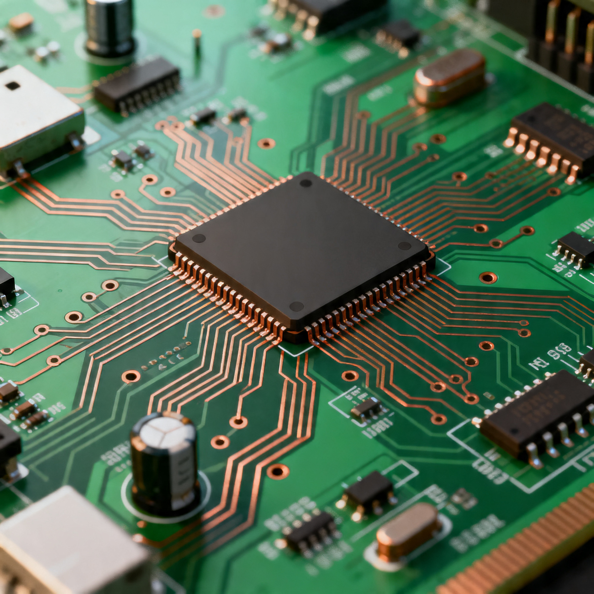
PCB design for high-performance applications involves a comprehensive understanding of the core concepts and architecture. At its heart, the architecture of a PCB is defined by its layers, traces, vias, and pads, which together form the pathways for electrical signals. The principles of signal integrity, thermal management, and electromagnetic compatibility (EMC) are crucial for maintaining the board's performance. High-frequency designs, particularly those involving RF components, require precise impedance control and careful consideration of parasitic effects. Engineers must also consider the dielectric properties of the substrate material, which affects signal propagation speed and loss. The integration of these elements into a cohesive design ensures that the PCB can handle the desired electrical requirements while maintaining reliability and efficiency.
Detailed Specifications
When designing a high-performance PCB, understanding the key specifications of components is paramount. These specifications, often detailed in datasheets, provide insights into the component's capabilities and limitations. Parameters such as operating frequency, power handling, and thermal resistance are crucial for selecting the appropriate components for your design. The following table outlines the key specifications for RF components commonly used in advanced PCB designs.
| Specification | Parameter | Value |
|---|---|---|
| Operating Frequency | GHz | 0.1 - 10 |
| Power Handling | Watts | 1 - 100 |
| Voltage Rating | Volts | 50 - 300 |
| Thermal Resistance | °C/W | 0.5 - 2.0 |
| Impedance | Ohms | 50 |
| Insertion Loss | dB | 0.1 - 1.0 |
| Return Loss | dB | 10 - 30 |
| Isolation | dB | 20 - 60 |
| Capacitance | pF | 0.1 - 2.0 |
| Inductance | nH | 0.1 - 10 |
| Dielectric Constant | - | 2.2 - 4.5 |
Key Takeaways from the Specifications
The data presented in Table 1 highlights the critical specifications that must be considered when selecting RF components for high-performance PCB designs. Operating frequency and power handling are primary considerations, as they dictate the component's suitability for specific applications. Thermal resistance and voltage rating are crucial for ensuring reliability under varying operating conditions. Impedance matching, as indicated by the uniform 50 Ohm standard, is vital for minimizing signal reflection and loss. Insertion and return loss metrics provide insights into the efficiency of signal transmission and reflection, respectively. Understanding these specifications allows engineers to make informed decisions and optimize their designs for performance and reliability.
| Performance Metric | Parameter | Value |
|---|---|---|
| Signal Integrity | Eye Diagram | Clear |
| Thermal Management | Junction Temperature | 85°C Max |
| EMC Compliance | EMI Reduction | 10 dB |
| Power Efficiency | Efficiency | 90% |
| Cross-Talk | dB | -40 |
| Noise Figure | dB | 1.5 |
| Gain | dB | 20 |
| Bandwidth | MHz | 500 |
| Phase Noise | dBc/Hz | -110 |
| Linearity | IP3 | 30 dBm |
Practical Implications
The performance metrics outlined in Table 2 are essential for evaluating the real-world behavior of RF components within a PCB design. Signal integrity is crucial for ensuring that data is transmitted accurately, with clear eye diagrams indicating minimal distortion. Effective thermal management, demonstrated by the junction temperature, ensures reliability and longevity. EMC compliance metrics, such as EMI reduction, are vital for minimizing interference with other electronic systems. Power efficiency and cross-talk values reflect the component's ability to operate effectively and minimize energy loss. These metrics provide a comprehensive understanding of the component's performance, guiding engineers in optimizing their PCB designs for high-frequency applications.
| Use Case | Configuration | Application |
|---|---|---|
| Wireless Communication | 2x2 MIMO | Wi-Fi Routers |
| Signal Amplification | Single-ended | RF Amplifiers |
| Frequency Conversion | Mixers | Transceivers |
| Filtering | Band-pass | RF Filters |
| Oscillation | Colpitts Oscillator | Signal Generators |
| Impedance Matching | LC Network | Antenna Systems |
| Power Distribution | Star Topology | Power Grids |
| Data Transmission | Serial Communication | Modems |
Application Guidelines
Table 3 provides a matrix of common use cases and configurations for RF components in PCB designs. Each configuration is tailored for specific applications, such as wireless communication, signal amplification, and frequency conversion. For instance, a 2x2 MIMO configuration is ideal for Wi-Fi routers, enhancing data throughput and connectivity. Single-ended configurations are suited for RF amplifiers, focusing on signal strength and clarity. Understanding these applications allows engineers to select the appropriate configuration for their design, ensuring optimal performance and functionality. These guidelines serve as a practical reference for integrating RF components into various electronic systems.
Design Considerations
Designing high-performance PCBs requires careful consideration of several factors to ensure optimal functionality and reliability. First, signal integrity must be prioritized through proper trace routing, impedance matching, and minimizing parasitic effects. This involves strategic placement of components and careful design of the PCB stack-up to maintain consistent impedance. Thermal management is another critical aspect, requiring the use of thermal vias, heat sinks, and appropriate substrate materials to dissipate heat effectively. Additionally, EMC considerations should be addressed by employing shielding techniques and filtering components to reduce electromagnetic interference. The choice of substrate material, such as FR-4 or Rogers, impacts the board's dielectric properties and can influence signal speed and attenuation. Finally, the use of simulation tools can aid in predicting the board's performance and identifying potential issues before fabrication. By integrating these considerations into the design process, engineers can create robust and efficient PCBs capable of meeting the demands of high-performance applications.
Step-by-Step Implementation
Implementing a high-performance PCB design involves several methodical steps to ensure success:
- Define Requirements: Begin by outlining the specific requirements of the PCB, including operating frequency, power levels, and environmental conditions.
- Component Selection: Choose components based on the specifications outlined in datasheets, ensuring compatibility with the desired application.
- Layout Design: Create the PCB layout, focusing on optimal trace routing, placement of components, and minimizing parasitic inductance and capacitance.
- Simulate the Design: Use simulation tools to analyze signal integrity, thermal performance, and EMC compliance, making adjustments as necessary.
- Prototype Fabrication: Fabricate a prototype of the PCB to test its real-world performance, identifying any discrepancies with the design.
- Testing and Validation: Conduct thorough testing to validate the PCB's performance against the defined requirements, focusing on key metrics such as signal integrity and thermal management.
- Iterative Improvement: Iterate on the design, making necessary adjustments based on test results to optimize performance and reliability.
- Final Production: Once validated, proceed with mass production, ensuring quality control measures are in place to maintain consistency.
Common Issues & Solutions
Despite meticulous planning, several common issues can arise during PCB design and manufacturing. Here are some typical problems and their solutions:
- Signal Reflection: Occurs due to impedance mismatches. Solution: Ensure proper impedance matching through trace width and spacing adjustments.
- Thermal Overload: Components overheating. Solution: Implement effective thermal management strategies, such as heat sinks and thermal vias.
- Electromagnetic Interference (EMI): Interference with other devices. Solution: Use shielding and filtering techniques to mitigate EMI.
- Cross-Talk: Unwanted coupling between traces. Solution: Maintain adequate spacing between traces and use ground planes for isolation.
- Manufacturing Defects: Issues like solder bridges. Solution: Adhere to IPC standards and conduct thorough inspections during manufacturing.
- Component Failure: Due to incorrect ratings. Solution: Carefully review datasheets and select components with appropriate specifications.
Applications & Use Cases
High-performance PCBs are integral to a wide range of applications across various industries. In telecommunications, they are used in base stations and antennas for reliable signal transmission. In the automotive sector, advanced PCBs are found in radar and communication systems, enhancing vehicle safety and connectivity. Consumer electronics, such as smartphones and tablets, rely on high-performance PCBs for efficient processing and wireless communication. In industrial automation, PCBs facilitate precise control and monitoring of machinery. These use cases underscore the versatility and importance of high-performance PCB designs in modern technology.
Selection & Sourcing Guide
Selecting and sourcing components for high-performance PCBs requires careful consideration of specifications and availability. Engineers should utilize resources like IC Online to access comprehensive databases of electronic components, ensuring that the selected parts meet the necessary performance criteria and are available for procurement. Collaborating with reputable suppliers and manufacturers is essential for securing high-quality components and maintaining the integrity of the PCB design.
FAQ
- What is the importance of impedance matching in PCB design?
Impedance matching is crucial for minimizing signal reflection and ensuring efficient signal transmission across the PCB. - How can I improve thermal management in my PCB design?
Utilize thermal vias, heat sinks, and appropriate substrate materials to effectively dissipate heat and prevent component overheating. - What are the common causes of EMI in PCBs?
EMI can be caused by poor shielding, improper grounding, and inadequate filtering. Addressing these issues can help reduce interference. - How do I select the right substrate material for my PCB?
Consider the dielectric properties, cost, and thermal characteristics of materials like FR-4 or Rogers to match the needs of your application. - Why are simulation tools important in PCB design?
Simulation tools allow engineers to predict the performance of the PCB, identify potential issues, and make necessary adjustments before fabrication. - What steps should I take to ensure signal integrity?
Focus on proper trace routing, impedance control, and minimizing parasitic effects to maintain signal integrity. - How can I prevent cross-talk in my PCB design?
Maintain adequate spacing between traces and use ground planes to isolate signals and reduce cross-talk. - What are the benefits of following IPC standards in PCB manufacturing?
IPC standards ensure quality and reliability by providing guidelines for design, assembly, and inspection processes. - How do I address component failure in my PCB?
Carefully review datasheets and select components with appropriate ratings to prevent failures due to incorrect specifications. - What role do application circuits play in PCB design?
Application circuits provide practical examples of how components can be configured and used in real-world applications, guiding engineers in their design process.
Conclusion
Designing high-performance PCBs is a complex yet rewarding endeavor that requires a deep understanding of component specifications, performance metrics, and application guidelines. By avoiding common pitfalls and adhering to best practices, engineers can create robust and efficient designs that meet the demands of modern technology. With the right tools, resources, and knowledge, the path to successful PCB design is both achievable and essential for advancing electronic innovation.