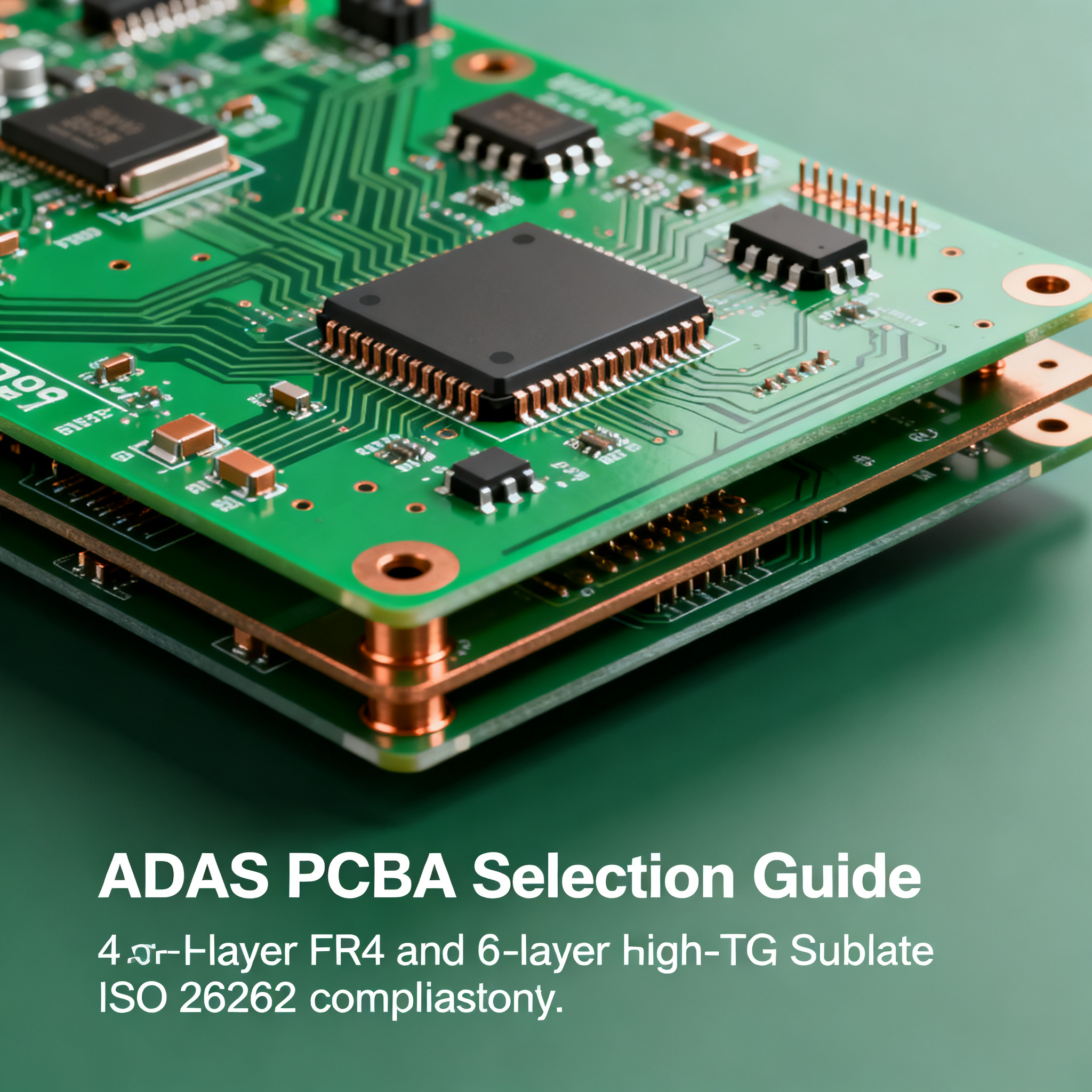
ADAS PCBA Selection Guide: Comparing 4-Layer FR4 vs. 6-Layer High-Tg Substrates for ISO 26262 Compliance
Why ADAS PCB Reliability Now Hinges on Substrate Selection ADAS modules have moved far beyond simple parking sensors. Today’s sensor-fusion ECUs pack high-resolution cameras, 4D imaging radar, and lid...
Why ADAS PCB Reliability Now Hinges on Substrate Selection
ADAS modules have moved far beyond simple parking sensors. Today’s sensor-fusion ECUs pack high-resolution cameras, 4D imaging radar, and lidar processors onto a single board, often mounted in thermally hostile zones—behind the grille, inside the headlamp housing, or directly on the engine bulkhead. Under these conditions, the PCB substrate is no longer just a mechanical carrier; it becomes the first line of defense against field failures that can cascade into safety incidents.
Field data from automotive Tier‑1 suppliers shows that thermal cycling between -40°C and +125°C, combined with vibration and humidity, can induce via cracking and conductive anodic filament (CAF) growth in conventional FR‑4 boards within 800–1,200 cycles. Once a via barrel fractures or a CAF path bridges adjacent nets, the ADAS function degrades—often without warning. These failure modes are precisely what IPC‑A‑610 Class 3 acceptance criteria seek to eliminate, but achieving Class 3 reliability on a standard 4‑layer FR‑4 stack is becoming increasingly difficult as signal speeds climb and package densities rise.
The shift toward high‑Tg (glass transition temperature ≥170°C) laminates and higher layer counts is not a marketing trend; it is an engineering necessity driven by the physics of thermal expansion and high‑speed signal propagation. At Nova PCBA, our high‑reliability assembly line has seen a 40% increase in ADAS projects specifying 6‑layer high‑Tg stacks over the last two years, reflecting a clear industry pivot. This guide examines why that pivot matters, how layer count and Tg interact with signal integrity and thermal endurance, and what the selection means for ISO 26262 compliance.
How Layer Count and Glass Transition Temperature Shape Signal Integrity and Thermal Endurance
Moving from a 4‑layer to a 6‑layer board adds more than routing real estate. It enables contiguous reference planes that dramatically improve the power delivery network (PDN) impedance and reduce crosstalk between high‑speed differential pairs. In ADAS designs, MIPI CSI‑2 lanes running at 1.5 Gbps or more need a solid ground plane directly adjacent to the signal layer to maintain characteristic impedance within ±10%. A 4‑layer stack often forces signal layers to share a single internal plane, creating split‑plane crossings and return path discontinuities that degrade eye diagrams and increase bit error rates.
High‑Tg substrates address a different but equally critical set of problems. Standard FR‑4 (Tg ≈130–140°C) exhibits a coefficient of thermal expansion (CTE) in the Z‑axis of 50–70 ppm/°C above Tg. During reflow soldering and subsequent thermal cycling, this expansion stresses plated through‑holes, leading to barrel cracks and pad lifting. A high‑Tg laminate like Isola’s IS410 (Tg 180°C) reduces Z‑axis CTE to 35–45 ppm/°C and raises the decomposition temperature, giving vias a much larger safety margin. Additionally, high‑Tg resins resist CAF growth better because they maintain higher insulation resistance under bias in hot, humid conditions—a key requirement for modules that operate in the engine compartment.
The table below compares key material parameters that directly influence ADAS PCB performance. Design rule references from IPC‑2221 guide minimum conductor spacing and via aspect ratios, but the substrate’s intrinsic properties set the ultimate reliability ceiling.
| Parameter | Standard FR‑4 (Tg 140°C) | High‑Tg FR‑4 (e.g., IS410, Tg 180°C) | Impact on ADAS Reliability |
|---|---|---|---|
| Glass Transition Temperature (Tg) | 130–140°C | 170–180°C | Higher Tg delays resin softening during reflow and thermal cycling, preserving via integrity. |
| Z‑axis CTE (below Tg) | 50–70 ppm/°C | 35–45 ppm/°C | Lower CTE reduces stress on plated through‑holes, cutting barrel crack risk by >50%. |
| Dielectric Constant (Dk) @ 1 GHz | 4.3–4.6 | 3.8–4.2 | Lower Dk allows thinner dielectrics for controlled impedance, saving space and reducing crosstalk. |
| Dissipation Factor (Df) @ 1 GHz | 0.018–0.022 | 0.012–0.016 | Lower loss tangent improves signal integrity for long MIPI or SerDes traces above 2 Gbps. |
| Thermal Conductivity | 0.3–0.4 W/m·K | 0.4–0.5 W/m·K | Slightly better heat spreading helps dissipate heat from processors, reducing hot spots. |
| CAF Resistance (85°C/85% RH, 100 V bias) | Failure often <500 h | Typically >1,000 h | High‑Tg resins suppress filament growth, critical for long‑term field reliability in humid environments. |
| Decomposition Temperature (Td) | 310–320°C | 340–350°C | Higher Td provides headroom during multiple reflow cycles and rework, preventing delamination. |
Tip: When simulating PDN impedance for a 6‑layer high‑Tg board, use the actual Dk and Df values from the laminate supplier’s datasheet, not generic FR‑4 numbers. The difference can shift the resonant peak by 200 MHz, which matters when you’re targeting a flat impedance profile up to 1 GHz for an ADAS SoC.
Layer count and Tg are not independent levers. A 6‑layer board built on standard FR‑4 still suffers from the same CTE and CAF weaknesses, just with better signal integrity. Conversely, a 4‑layer high‑Tg board improves thermal endurance but may lack the reference plane quality needed for high‑speed signals. The next section compares these two configurations head‑to‑head for typical ADAS use cases.
4‑Layer FR4 vs. 6‑Layer High‑Tg: A Direct Comparison for ADAS Modules
Choosing between a 4‑layer FR‑4 and a 6‑layer high‑Tg stack is not simply a cost decision; it is a functional safety trade‑off that determines the module’s usable life, signal fidelity, and compliance ceiling. The table below distills the key differentiators, followed by real‑world ADAS examples that illustrate where each configuration fits—and where it breaks.
| Comparison Metric | 4‑Layer FR‑4 (Tg 140°C) | 6‑Layer High‑Tg (Tg 180°C) | Selection Criteria & Failure Boundary |
|---|---|---|---|
| Typical Cost per sq. inch (production volume) | $0.15–$0.25 | $0.35–$0.55 | Cost delta of 30–60%; justified when field failure risk outweighs BOM savings. |
| Stackup Example | Signal‑GND‑PWR‑Signal | Signal‑GND‑Signal‑PWR‑GND‑Signal | 6‑layer provides two solid reference planes, eliminating split‑plane crossings for high‑speed signals. |
| Impedance Control Tolerance | ±12–15% typical | ±8–10% achievable | Tighter tolerance needed for MIPI lanes above 1 Gbps; 4‑layer often fails eye mask at 1.5 Gbps. |
| Crosstalk (near‑end, 100 mil spacing) | ‑25 dB to ‑20 dB | ‑35 dB to ‑30 dB | 6‑layer with adjacent ground planes reduces crosstalk by 10 dB, critical for parallel sensor interfaces. |
| Thermal Cycles to Failure (‑40°C to +125°C, IPC‑9701) | 800–1,200 cycles | 2,000–3,000+ cycles | ASIL C/D modules require >2,000 cycles; 4‑layer FR‑4 falls short without heavy derating. |
| Via Aspect Ratio Limit (reliable) | 8:1 | 10:1 | 6‑layer high‑Tg supports smaller vias for dense BGAs without compromising barrel integrity. |
| Suitable ADAS Functions | Blind‑spot detection, simple parking sensors, low‑speed CAN nodes | Forward‑facing cameras, radar/lidar fusion, automated emergency braking, domain controllers | Match function to ASIL level; ASIL B and above almost always require 6‑layer high‑Tg. |
| Assembly Process Sensitivity | Standard reflow; low warpage risk | Requires tight profile control, pre‑bake, and vacuum lamination to avoid outgassing | Experienced assemblers like Nova PCBA compensate with optimized thermal profiles, maintaining first‑pass yield >98%. |
Consider a blind‑spot detection radar operating over a single CAN‑FD link with a modest 2‑layer RF front‑end. A 4‑layer FR‑4 board can handle the digital processing and power management reliably, and the module’s location in the rear bumper corners exposes it to moderate thermal swings. Here, the cost savings are real and the reliability margin is acceptable for ASIL A/B with proper design derating.
Now contrast that with a forward‑facing camera module processing 8‑megapixel images over four MIPI CSI‑2 lanes at 1.5 Gbps each. The image sensor and processor sit on a dense BGA package with 0.5 mm pitch, requiring microvias and tight impedance control. The module is mounted behind the windshield, where solar soak can push ambient temperatures above 105°C. In this scenario, a 4‑layer FR‑4 board would suffer from degraded signal eyes, via fatigue within 1,000 thermal cycles, and a high probability of CAF‑induced leakage. A 6‑layer high‑Tg stack with two solid ground planes and a dedicated power plane not only meets the signal integrity budget but also provides the thermal endurance to survive 15‑year vehicle life. Nova PCBA’s assembly process for such boards includes extended pre‑bake at 125°C for 8 hours, vacuum lamination to eliminate moisture, and a reflow profile with a controlled soak zone to prevent outgassing and warpage on high‑Tg laminates.
ISO 26262 and the Case for High‑Tg Substrates in Safety‑Critical ADAS
ISO 26262 functional safety standard imposes a rigorous development process that extends all the way to the PCB substrate. For ASIL C and D systems—such as automatic emergency braking or lane‑keeping assist—the safety case must demonstrate that the hardware can meet the required failure‑in‑time (FIT) rates and survive the mission profile without systematic or random hardware failures. The PCB substrate directly influences three pillars of that safety case: thermal endurance, insulation integrity, and traceability.
High‑Tg laminates support the extended temperature cycling profiles mandated by the automotive safety integrity level. A typical ASIL D validation plan includes 2,000–3,000 thermal cycles from -40°C to +125°C with continuous electrical monitoring. Standard FR‑4 boards begin to show via resistance shifts and intermittent opens well before 1,500 cycles, which would violate the quantitative reliability target. High‑Tg materials, with their lower Z‑axis CTE and higher decomposition temperature, keep via resistance stable beyond 3,000 cycles, providing the margin needed to satisfy the safety case.
CAF resistance is equally critical. A single conductive filament bridging two nets can create a latent fault that escapes end‑of‑line test and manifests only after months in the field. ISO 26262 requires that such failure modes be addressed by design or by a dedicated safety mechanism. Using a high‑Tg laminate with proven CAF resistance (typically >1,000 hours at 85°C/85% RH under bias) is a design measure that reduces the risk of insulation breakdown to an acceptable level. Qualification testing per IPC‑6012 Class 3 and IPC‑A‑610 Class 3 acceptance criteria then verifies that the manufactured board meets those design intents.
Traceability is the third leg. ISO 26262 demands full material lot traceability from laminate supplier to finished assembly, so that any field returns can be traced back to the specific production batch. Nova PCBA’s quality system assigns a unique serialized work order to each PCB lot, logs every laminate batch number, and records in‑line AOI/SPI data for every board. This granular data package becomes part of the safety case documentation, demonstrating that the manufacturing process was under control and that no unverified material entered the production stream.
The table below maps key ISO 26262 safety requirements to substrate properties and shows how a 6‑layer high‑Tg board satisfies them more robustly than a 4‑layer FR‑4 alternative.
| ISO 26262 Safety Requirement | Substrate Property That Addresses It | 4‑Layer FR‑4 Performance | 6‑Layer High‑Tg Performance |
|---|---|---|---|
| Extended thermal cycling endurance (ASIL C/D) | Z‑axis CTE, Tg, Td | Marginal beyond 1,200 cycles; via cracking likely | Reliable beyond 2,500 cycles; stable via resistance |
| Insulation resistance under humidity & bias | CAF resistance, resin chemistry | CAF failures possible <500 h; risk of latent shorts | CAF‑resistant resin; >1,000 h without failure |
| Signal integrity for safety‑critical data paths | Dk, Df, layer stackup with solid reference planes | Split‑plane crossings degrade eye; higher BER | Contiguous ground planes; tight impedance control |
| Material lot traceability | Laminate batch marking, supply chain control | Possible but often not enforced for low‑cost builds | Standard practice for safety‑critical assemblies; full traceability from supplier to finished board |
| Resistance to tin whisker growth (Pb‑free) | Surface finish compatibility, CTE mismatch | Higher CTE mismatch can stress solder joints, promoting whiskers | Lower CTE reduces stress; ENIG/ENIPIG finishes further mitigate risk |
Note: While a 6‑layer high‑Tg board provides inherent advantages, the safety case still requires verification testing on the actual production design. Nova PCBA supports customers with thermal stress testing, microsection analysis, and CAF coupon data that feed directly into the ISO 26262 work products.
ADAS Substrate Decisions: Questions Engineers and Buyers Ask
Q: At what point does a 4‑layer FR4 board become inadequate for an ADAS application?
A 4‑layer FR‑4 board becomes inadequate when the design requires high‑speed differential pairs (e.g., MIPI CSI‑2 above 1 Gbps), dense BGA packages with 0.5 mm pitch or finer, or must survive more than 1,000 thermal cycles from -40°C to +125°C. The lack of continuous reference planes and the lower Tg typically make 4‑layer FR‑4 unreliable for ASIL B and above. Once you need controlled impedance within ±10% on multiple lanes, a 6‑layer high‑Tg stack is the practical minimum.
Q: How does high‑Tg material affect PCB assembly yield?
High‑Tg laminates require tighter control of reflow profiles to avoid outgassing and delamination. The higher curing temperature of the resin means that moisture absorbed during storage must be driven out with an extended pre‑bake (typically 8–12 hours at 125°C). Experienced manufacturers like Nova PCBA compensate with vacuum lamination, optimized soak zones, and nitrogen reflow to keep first‑pass yield comparable to standard FR‑4—often above 98% for well‑designed panels. The key is to involve the assembly partner early in the DFM review to adjust pad geometries and panelization for the higher‑Tg material’s slightly different expansion behavior.
Q: What is the typical cost delta between 4‑layer FR4 and 6‑layer high‑Tg for an ADAS ECU?
A 6‑layer high‑Tg board can cost 30–60% more than a 4‑layer FR‑4 of the same size, driven by additional material, lamination cycles, and tighter process controls. However, the per‑unit cost is often offset by reduced field failures and warranty claims in safety‑critical functions. When you factor in the cost of a single automotive recall, the upfront premium becomes negligible. Many Tier‑1 suppliers treat the 6‑layer high‑Tg as the baseline for any ADAS module with ASIL B or higher.
Q: Can I use a hybrid stackup with FR4 and high‑Tg layers to balance cost and performance?
Hybrid constructions are possible but introduce CTE mismatch risks that can lead to warpage or via failure during reflow. The different expansion rates of the core and prepreg layers create internal shear stresses that concentrate at the via barrels. For ADAS, a monolithic high‑Tg stack is generally recommended unless the design has been thoroughly validated through thermal cycling and CAF testing. If you must use a hybrid, limit the high‑Tg layers to the outer layers and keep the aspect ratio below 6:1, but expect to invest significant effort in qualification.
Q: What IPC class is required for ADAS PCBs?
Most ADAS modules fall under IPC‑A‑610 Class 3 (high‑performance electronics) due to the life‑safety implications. This class demands tighter annular ring requirements, minimal voiding in solder joints, and more rigorous inspection criteria. Achieving Class 3 is easier on a 6‑layer high‑Tg substrate because the material’s dimensional stability and lower CTE help maintain registration and via integrity through multiple thermal excursions. Class 2 is sometimes accepted for non‑safety ADAS functions like parking assist, but any system that can influence braking, steering, or driver warning must meet Class 3.
Q: How does Nova PCBA ensure ISO 26262 traceability in manufacturing?
Nova PCBA implements full material lot traceability from laminate supplier to finished board, in‑line AOI/SPI data logging, and serialized work orders that link every assembly step to the specific PCB batch. Each board receives a unique 2D barcode that ties back to the laminate lot, solder paste batch, and reflow profile used. This data package supports the safety case documentation required for ASIL‑compliant ADAS systems and enables rapid root‑cause analysis if a field return occurs.
References & Further Reading
- IPC‑A‑610 Acceptability of Electronic Assemblies – IPC
- IPC‑2221 Generic Standard on Printed Board Design – IPC
- IPC‑6012 Qualification and Performance Specification for Rigid Printed Boards – IPC
- Nova PCBA – Professional PCB Assembly Services
- Nova PCBA – PCB Assembly Capabilities
- Nova PCBA – Quality Assurance & Traceability
- Isola IS410 High‑Tg Laminate Datasheet – Isola Group
- EE Times – Automotive Electronics Insights
- PCBWay – High‑Tg PCB Fabrication
Selecting the right substrate for an ADAS module is a multi‑dimensional decision that balances signal integrity, thermal endurance, functional safety, and cost. While a 4‑layer FR‑4 board still serves simple, low‑speed sensor nodes, any design that touches high‑speed data paths or ASIL B+ safety goals should default to a 6‑layer high‑Tg stack. The upfront material premium is consistently outweighed by the reduction in field failures and the confidence it brings to the ISO 26262 safety case. Partnering with an assembly provider that understands the nuances of high‑Tg processing—from pre‑bake to final inspection—ensures that the design intent translates into reliable hardware. At Nova PCBA, we combine deep experience in automotive‑grade assembly with the traceability and process controls that ADAS programs demand, helping you deliver boards that perform safely over the vehicle’s entire life.