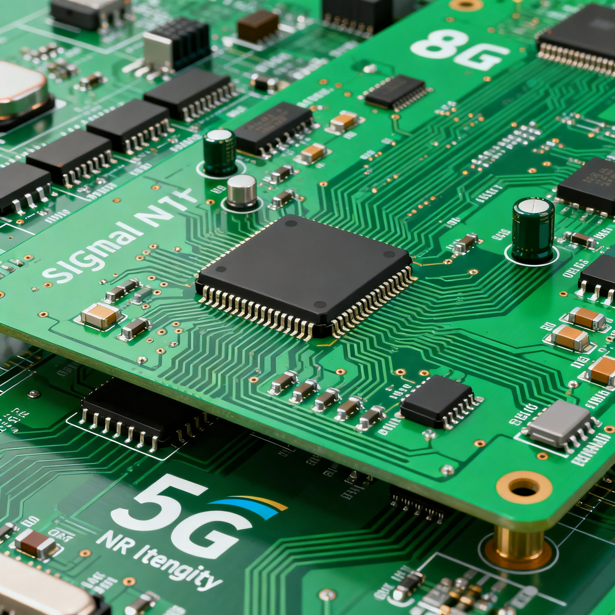
Achieving 5G NR Signal Integrity in 8-Layer Communication PCB Assembly for 2026 Deployments
When Expired Test Instruments Meet mmWave: Why 5G NR PCB Assembly Demands More Than a Pass/Fail Report A factory floor filled with imported vector network analyzers and time-domain reflectometers can ...
When Expired Test Instruments Meet mmWave: Why 5G NR PCB Assembly Demands More Than a Pass/Fail Report
A factory floor filled with imported vector network analyzers and time-domain reflectometers can project an image of precision—until you discover that the calibration standards used to verify those instruments expired six months ago. That was the unsettling reality shared by engineers who visited a 5G antenna board supplier, as documented in a Sprintpcbgroup field report. The lab’s reports looked flawless, yet the boards later exhibited intermittent phase errors and insertion loss drift at 28 GHz. The culprit wasn’t the laminate or the design; it was a measurement chain that had drifted out of tolerance, masking critical signal integrity deviations.
This story crystallizes a deeper tension that the research community is now openly acknowledging: it is difficult to achieve nice signal integrity and reliability simultaneously in 5G millimeter-wave PCB assemblies. An Emerald Microelectronics International investigation into new reliability issues of PCBs in 5G mmWave applications highlights that the same physical features engineered for low loss—smooth copper, thin dielectrics, precise backdrilling—can introduce latent failure modes under thermal cycling and high humidity. For 2026 deployments, where 5G NR networks will densify with small cells, massive MIMO arrays, and private industrial radios, the 8-layer PCB has become the de facto baseline. It offers the shielding, impedance control, and power integrity headroom that a 6-layer stackup cannot reliably sustain beyond 10 GHz. But the assembly ecosystem must mature: pass/fail testing without verified metrology is a liability you cannot afford.
This article unpacks the 8-layer playbook for 5G NR signal integrity, from stackup physics and dielectric selection to backdrilling tolerances and collaborative DFM, so you can ship boards that perform in the field—not just on a questionable test report.
The 8-Layer Stackup Playbook for 5G NR: Impedance Targets, Dielectrics, and the Ground Plane Shield
The 5G NR physical layer, defined in ETSI TS 138 201, operates across two frequency ranges: FR1 (sub-6 GHz) and FR2 (24.25–52.6 GHz). The channel structure—spanning the physical downlink shared channel, uplink control, and sounding reference signals—demands tightly controlled impedance and low phase noise. A practical deep-dive into 5G NR channels and physical layer processing underscores that even a 2 dB ripple in the transmission line can degrade error vector magnitude (EVM) below the 3.5% target for 64QAM. An 8-layer stackup provides the multiple ground planes and thin signal-to-reference dielectrics needed to hit these numbers.
The table below prescribes a proven 8-layer configuration for mixed-signal 5G NR boards, balancing FR2 performance with FR1 robustness. It draws on stackup guidelines from Allpcb’s 8-layer signal integrity guide and Aivon’s ground plane strategies, both aligned with IPC-2221B.
| Layer | Function | Material / Dk (Typ.) | Thickness (mil) | Trace Width for 50 Ω Single-Ended (mil) |
|---|---|---|---|---|
| 1 (Top) | RF/Analog Signals (FR2) | Rogers RO3003 / 3.00 | 5.0 | 12.0 |
| 2 | Ground Plane (GND) | 1 oz. Cu, prepreg | — | — |
| 3 | High-Speed Digital (FR1/DDR5) | Megtron 6 / 3.40 | 4.0 | 4.8 |
| 4 | Ground Plane (GND) | 1 oz. Cu, core | — | — |
| 5 | Power Plane (VDD) | 1 oz. Cu, core | — | — |
| 6 | Ground Plane (GND) | 1 oz. Cu, prepreg | — | — |
| 7 | Low-Speed Digital / Control | Megtron 6 / 3.40 | 4.0 | 4.8 |
| 8 (Bottom) | RF/Analog Signals (FR2) & Test | Rogers RO3003 / 3.00 | 5.0 | 12.0 |
This stackup sandwiches every signal layer between two adjacent ground planes, maximizing isolation and providing a deterministic return path. The dielectric thickness between Layer 1 and Layer 2 is only 5 mil, which keeps the impedance tolerance within ±7% even with standard etching variation—a critical requirement when you’re working with a manufacturer on a controlled-impedance coupon. The Rogers RO3003 material on the outer layers yields a Dk of 3.00 ±0.04 and a loss tangent of 0.0010, keeping conductor losses manageable at 39 GHz. Inner digital layers rely on Megtron 6 (Dk 3.4, Df 0.002) for high-speed DDR5 lanes while still supporting sub-6 GHz RF paths if needed.
Tip: When you specify this stackup, request a TDR verification of the impedance test coupon from the same panel, not a generic witness coupon. Coupon-to-board variation can be as high as 3–5 Ω if the fabricator alters the prepreg type without notifying you.
Via stubs are the silent killer of FR2 signal integrity. Any unused portion of a plated through-hole via acts as a quarter-wave stub, causing a deep notch in insertion loss. For 28 GHz, the resonant stub length is roughly 80 mils in Megtron 6; even a 20-mil stub can introduce a 3 dB dip. You must backdrill all vias on FR2 signal paths to a residual stub length of less than 10 mils (0.25 mm). The 8-layer design allows you to route the RF signals on the outer layers and backdrill from the opposite side, removing the stub entirely. Crosstalk reduction is equally rigorous: maintain a minimum line-to-line spacing of 3× the dielectric height for parallel runs longer than 500 mils, and use guard traces tied to GND with vias every 200 mils on sensitive clock lines.
6-Layer vs 8-Layer: When the Cost Premium Pays for 5G NR Signal Integrity
The decision to move from 6 to 8 layers is often framed as a cost question, but the real metric is the dielectric distance between your signal trace and its immediate reference plane. As QueenEMS’s 6-layer vs 8-layer analysis emphasizes, that distance dictates impedance stability far more than total board thickness. In a 6-layer stackup, you typically have only two dedicated ground planes and must route high-speed signals on layers that share a reference with a split power plane, leading to impedance discontinuities at plane transitions. An 8-layer board gives you four solid ground planes and dedicated power planes, enabling a stripline configuration for critical digital buses and a clean microstrip or grounded coplanar waveguide for mmWave RF.
The cost delta is real but contextual. JHYPCB’s cost-performance comparison notes that prototypes cost 30–50% more than 6-layer equivalents; in volume, the premium drops to 20–35%, depending on size, via count, and finish. For 5G NR radios operating above 10 GHz, that premium often pays for itself in first-pass yield and field reliability. WonderfulPCB’s 8-layer design guide further confirms that 8 layers are mandatory for server motherboards, AI accelerator cards, and GPU boards with DDR5 memory, where multiple power planes and stringent signal integrity margins leave no room for a 6-layer compromise.
The table below compares the two architectures against the specific demands of 5G NR communication assemblies.
| Comparison Metric | 6-Layer Rigorous Design (Hybrid) | 8-Layer 5G NR Optimized | Selection Criteria & Failure Boundary |
|---|---|---|---|
| Max usable frequency with ±10% impedance tolerance | ~10 GHz (with thin dielectrics and tight coupling) | ≥39 GHz with proper backdrilling | If your board includes FR2 carriers (28/39 GHz), 6 layers is insufficient for consistent impedance. |
| Number of dedicated ground planes | 2 (must share with split power) | 4 (each signal layer adjacent to unbroken GND) | Mixed-signal crosstalk on 6 layers often forces re-spin; 8 layers isolate RF, digital, and power. |
| Power plane integrity (PDN) | Single split plane, higher inductance | Dedicated power plane, low inductance | DDR5 and 5G NR baseband processors demand target impedance <10 mΩ up to 100 MHz; 8 layers achieve this with plane capacitance. |
| Via stub mitigation | Backdrilling possible but limited by stack symmetry | Backdrill from bottom to remove all stubs on RF layers | FR2 stub length >10 mils creates notch filters; 8 layers allow full removal. |
| Volume cost premium over 6-layer (JHYPCB data) | Baseline | +20–35% (ENIG, controlled impedance) | If the BOM cost of a field failure exceeds $500/board, the premium is trivial. |
When your design includes a 5G NR radio unit with a massive MIMO antenna array, a baseband processor with DDR5, and a power management IC all on the same substrate, the 8-layer stackup stops being optional. The extra ground planes not only shield the sensitive RF channels from the digital noise of the 64-bit memory bus but also provide the thermal vias necessary to draw heat away from the power amplifier. A 6-layer board trying to accomplish the same would require a complex hybrid stackup with exotic dielectrics that may actually cost more than a standard 8-layer build with a mid-range low-loss laminate.
From Stackup Review to Assembly: How to Avoid the Signal Integrity Traps That Testing Alone Can't Catch
The 10 golden rules for signal integrity in 5G PCB design from iwdfsolutions underscore a principle that the expired calibration story made painfully clear: working with your PCB manufacturer from day one prevents design rework and cost surprises. The first four weeks of a project should follow a disciplined collaboration rhythm: Week 1–2 for stackup review and material availability confirmation, Week 3–4 for design rule definition and impedance target locking. Skipping this step invites the manufacturer to make unilateral substitutions that break your signal integrity budget.
Yet even with a perfect stackup, the eight signal integrity pitfalls catalogued by Protoexpress—impedance mismatches, insufficient trace spacing, via stubs, PDN noise, conductor losses, crosstalk, return path discontinuities, and fiber-weave effect—remain lurking. Here’s how to address them in the context of an 8-layer 5G NR assembly.
Trace Width Calculation and Impedance Verification
Once you’ve selected materials and defined your stackup geometry, calculate the trace width for single-ended and differential pairs using a 2D field solver, not a generic calculator. For the stackup in Table 1, a 5-mil dielectric with Rogers RO3003 yields a 12-mil-wide trace for 50 Ω. But if your fabricator substitutes a prepreg with a Dk of 3.35 instead of 3.00, the impedance drops to 46 Ω—a 8% shift that can cause a 2 dB return loss penalty. Insist on receiving the measured TDR plots for the impedance coupon on every panel, and compare them to your simulation. The Sprintpcbgroup incident could have been caught if the OEM had simply requested a copy of the calibration certificate and cross-checked the TDR data with a known gold standard.
PDN Noise Mitigation
Power distribution network noise is a primary source of jitter in the 5G NR baseband clock. The 8-layer stackup dedicates an entire plane (Layer 5) to VDD, sandwiched between two ground planes. This creates a low-inductance path and a plane capacitance of roughly 200 pF per square inch with a 4-mil core. Use a target impedance of 5 mΩ up to 50 MHz, achieved by placing decoupling capacitors (100 nF, 10 nF, 1 nF) directly adjacent to the BGA pads on the bottom side. Simulate the PDN with a tool like Ansys SIwave or Cadence Sigrity; the 8-layer arrangement typically reduces the first resonance peak by 40% compared to a 6-layer equivalent.
Backdrilling Specifications
For every via carrying an FR2 signal, create a dedicated backdrill layer in your fabrication notes. Specify the signal layers to be backdrilled, the maximum stub length (10 mils), and the minimum annular ring after backdrilling. A common mistake is to backdrill all vias on a net, but you only need to drill the unused portion on the layer opposite the signal launch. Share a backdrill specification file aligned with IPC-6012 addenda, and request a backdrill report per layer showing the measured stub depth using a cross-section microscope. This practice closes the loop between design intent and physical reality.
The table below summarizes the primary traps and their mitigation techniques, directly applicable to 8-layer 5G NR boards.
| Signal Integrity Trap | Root Cause | 8-Layer Mitigation Strategy | Verification Method |
|---|---|---|---|
| Impedance mismatch | Dk variation, etching tolerance | Specify ±7% impedance tolerance, use thin signal-to-GND dielectric | TDR on impedance coupon, per panel |
| Via stub resonance | Unused via barrel at FR2 frequencies | Backdrill to <10 mils, specify stub tolerance in fab notes | Backdrill cross-section report, VNA measurement of via chain |
| PDN noise | High loop inductance, insufficient decoupling | Dedicated power plane between two GND planes, local decoupling | Impedance analyzer sweep (1 kHz – 100 MHz) on PDN test coupon |
| Conductor losses | Skin effect, copper roughness at mmWave | Use smooth copper (VLP-2 or Rz < 2.5 µm) on RF layers | Insertion loss S-parameter measurement to 40 GHz |
| Return path discontinuity | Split reference planes, layer transitions | Every signal layer adjacent to full GND plane; stitching vias near transitions | 3D EM simulation (HFSS/CST) of critical nets; TDR on board |
Key Takeaway: Testing can confirm that a board meets a specification, but only a DFM process that embeds impedance control, backdrilling verification, and metrology integrity can guarantee that the board will survive the thermal and mechanical stresses of a 5G NR deployment. The expired calibration story is a reminder that you must verify the verifier.
Your Toughest 5G NR 8-Layer PCB Assembly Questions, Answered
Q: What dielectric materials (beyond standard FR4) do you recommend for 8-layer 5G NR boards operating at 28 GHz and 39 GHz?
For FR2 frequencies, you must move beyond standard FR4 whose Dk varies wildly and whose loss tangent can exceed 0.02. Low-loss laminates like Rogers RO3000 series (RO3003, RO3035) offer a Dk of 3.00 ±0.04 and a loss tangent of 0.0010 at 10 GHz, with stable performance through 77 GHz. For a hybrid stackup, use Rogers material on the outer RF layers and a low-loss mid-layer dielectric like Isola Astra MT77 (Dk 3.45, Df 0.0017) or Panasonic Megtron 6 (Dk 3.4, Df 0.002). Equally important is the copper foil: specify very low profile (VLP-2) or rolled copper with a surface roughness Rz below 2.5 µm to minimize conductor losses due to skin effect at mmWave. Pairing a smooth copper with a tight Dk tolerance resin ensures that your 50 Ω line stays within 2 Ω across the entire panel.
Q: How can I verify that my fabricator is maintaining impedance control if their calibration tools might be expired, as seen in the Sprintpcb story?
You cannot rely on a certificate of conformance alone. Request the most recent calibration certificates for all network analyzers and TDR equipment used for your job, and check the expiration date. Specify in your fabrication documentation that each panel must include an impedance test coupon located on the same panel, built with the same lamination cycle. Ask for the measured TDR plots (not just pass/fail data) with your shipment, and compare those plots to your simulation. Establish a periodic audit cycle: visit the fab or commission a third party to verify the calibration log and test a known standard board. Many OEMs are now adding a reference coupon with a golden impedance trace that they can measure independently upon receipt, acting as a final go/no-go gate.
Q: What is the realistic lead time for 8-layer communication PCBs with ENIG finish and controlled impedance in today's supply chain?
For prototypes, expect 2–3 weeks from the time the stackup is approved and materials are in stock. Volume production with ENIG finish and controlled impedance typically runs 4–6 weeks. However, if your design uses high-end materials like Megtron 6 or Rogers, lead times can extend by 1–2 weeks because many fabricators keep these laminates in limited inventory. The best way to avoid surprises is to engage the manufacturer during the stackup review phase (Week 1–2 of the design cycle) as recommended by the 5G PCB design golden rules. Locking in material availability and build slots before you finalize the layout saves downstream delays and prevents the shop from substituting a different prepreg that could shift your impedance.
Q: Is an 8-layer stackup always necessary for 5G NR sub-6 GHz, or can a 6-layer board with a hybrid stackup meet the signal integrity requirements?
Not always. A well-designed 6-layer board with a thin dielectric between the signal layer and its reference plane can handle frequencies up to approximately 10 GHz, as noted in the JHYPCB comparison. If your radio operates only in the 3.5 GHz band and you aren’t driving a massive MIMO array, a 6-layer hybrid with a low-loss outer layer and a solid ground plane can meet the specs. However, when you add a multi-channel digital baseband, DDR5 memory, and a separate power management plane, the 6-layer board loses the dedicated ground planes needed to isolate the analog front-end from digital noise. The 20–35% cost premium for an 8-layer board often pays for itself by eliminating the debugging hours and re-spins associated with marginal crosstalk and PDN noise.
Q: What via stub length should I specify for backdrilling on FR2 signals, and how do I communicate that to the PCB manufacturer?
For 28 GHz and above, keep the remaining stub length below 10 mils (0.25 mm). At 39 GHz, even 8 mils can cause a noticeable resonance, so aim for 5–6 mils if the registration capability allows. In your fabrication notes, identify the specific signal layers that need backdrilling (e.g., “Backdrill all vias on Layer 1 and Layer 8 that connect to inner layers, removing the stub from Layer 8 to Layer 7”). Specify the maximum stub tolerance and the required annular ring after backdrilling. Provide a backdrill specification file that maps each signal net to its backdrill depth, and request a backdrill report per layer with cross-section micrographs. This practice aligns with IPC-6012 addenda and gives you the documentation you need to correlate any field failures with manufacturing deviations.
At NovaPCBA, we integrate these signal integrity verification steps into every 5G NR assembly project. Our controlled-impedance manufacturing lines, calibrated metrology, and material traceability ensure that the 8-layer board you sign off on is the board you get—without the unpleasant surprises of expired calibration data or undocumented prepreg swaps. To explore how our assembly capabilities and engineering support can accelerate your 2026 deployment, visit NovaPCBA.
References & Further Reading
- Investigation on the new reliability issues of PCB in 5G millimeter wave application – Emerald Microelectronics International
- 5G NR Channels and Physical Layer Processing (2026 Deep-Dive Guide) – TelecomGurukul
- 8 Factors that Lead to Signal Integrity Issues in a PCB – Sierra Circuits
- Telecom Infrastructure PCB: Mastering High-Speed Signal Integrity and Long-Term Field Reliability – Sprintpcbgroup
- 8-Layer PCB Design Guide: Stack-up, Applications, and Cost Analysis – WonderfulPCB
- 6 Layer vs 8 Layer PCB: Is the Extra Cost Worth It for Your Design? – QueenEMS
- 6 Layer vs 8 Layer PCB: Cost, Performance and Complexity Compared – JHYPCB
- 10 Golden Rules for Signal Integrity in 5G PCB Design – iwdfsolutions
- Unlock Signal Integrity: The Ultimate Guide to 8 Layer PCB Stackup Design – Allpcb
- Unlock Signal Integrity: The Ultimate Guide to 8-Layer PCB Stackup Design – Aivon
- ETSI TS 138 201 V15.0.0 – 5G; NR; Physical layer; General description