AC-DC Power Converter PCB Assembly: 2026 Manufacturing Best Practices for 2oz Copper, High-Isolation Boards
Why 2oz Copper and High-Isolation Are No Longer Optional in AC-DC Power Converters The AC-DC power converter landscape in 2026 is defined by three relentless forces: escalating power densities, tighte...
Why 2oz Copper and High-Isolation Are No Longer Optional in AC-DC Power Converters
The AC-DC power converter landscape in 2026 is defined by three relentless forces: escalating power densities, tightening medical and industrial safety mandates, and the constant pressure to reduce total cost of ownership. A decade ago, 1oz copper and basic FR-4 isolation were adequate for many offline power supplies. Today, they are a liability. As converter outputs climb past 500W in shrinking footprints, thermal management and dielectric integrity have moved from afterthoughts to primary design constraints.
Consider the economics. Prototype quantities of a custom AC-DC converter PCB carry a significant per-unit premium—advanced processes like heavy copper etching and high-CTI laminates inflate NRE and unit costs. Yet, as King Sun PCB’s 2025 pricing guide confirms, bulk orders substantially reduce the price delta. This dynamic forces engineering teams to commit early to a robust platform: 2oz copper for current handling and thermal spreading, and isolation architectures that meet 2×MOPP (Means of Patient Protection) without consuming excessive board area. Waiting until the pilot build to discover that 1oz traces overheat or that creepage distances fail hipot testing is no longer an option.
Medical device manufacturers, in particular, have driven the shift. A recent project highlighted by Hilelectronic achieved 2×MOPP isolation in 40% less space by combining strategic slot placement with high-CTI materials. That kind of space savings directly translates to smaller enclosures and lower system cost—but only if the PCB assembly process can reliably produce 2oz copper boards with those isolation features. The manufacturing challenge, then, is not just about meeting a spec on paper; it’s about building thousands of units with repeatable creepage, consistent plating, and zero field failures due to tracking or delamination.
In this article, we’ll walk through the assembly best practices that make 2oz copper, high-isolation AC-DC converter PCBs manufacturable at scale. You’ll learn how to balance cost, performance, and reliability from prototype through volume production.
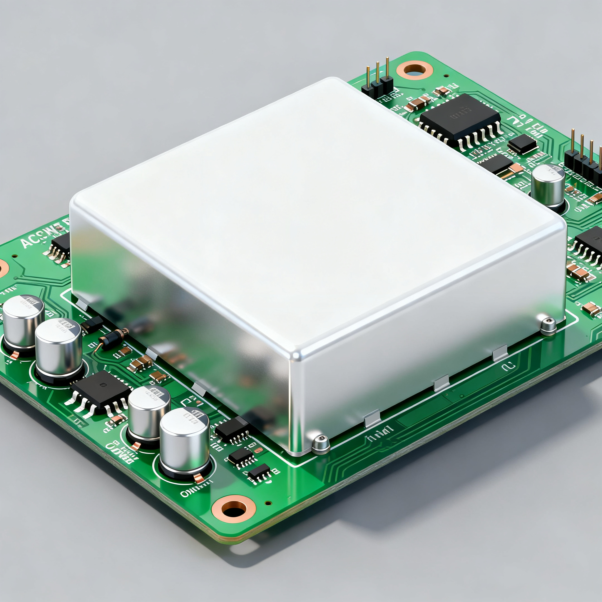
How 2oz Copper Traces and Isolation Slots Shape AC-DC Converter PCB Assembly
Moving from 1oz to 2oz copper fundamentally changes the PCB fabrication and assembly flow. Standard copper weights include 1oz (35 µm), 2oz (70 µm), and 3oz (105 µm), as noted by PCB HERO. Thicker copper increases current-carrying capacity but introduces etching undercut, plating non-uniformity, and thermal mass challenges during soldering. For AC-DC converters, where primary-side traces may carry several amps and secondary-side outputs demand low IR drop, 2oz is often the sweet spot—but only if the assembly process is tuned for it.
Below is a summary of the key process parameters that change when you specify 2oz copper for an AC-DC power converter PCB.
| Parameter | 1oz Copper (35 µm) | 2oz Copper (70 µm) | Assembly Impact |
|---|---|---|---|
| Minimum trace width/space (outer layers) | 4/4 mil typical | 6/6 mil or larger | Limits routing density; requires wider pad-to-trace transitions |
| Plating time (through-hole) | Baseline | 1.5–2× longer | Increases fabrication lead time; demands uniform current distribution |
| Etching undercut | Minimal | Noticeable; can reduce trace cross-section | Requires etch compensation in CAM; affects impedance control |
| Thermal mass during reflow | Low | High; slower ramp rates needed | Risk of tombstoning and cold joints if profile not adjusted |
| Solder paste volume | Standard stencil (4–5 mil) | Often requires step-up stencil or larger apertures | Ensures adequate solder fillet on heavy copper pads |
| Current capacity (10°C rise) | ~3.5 A for 100 mil width | ~7 A for 100 mil width | Enables compact power paths; reduces I²R losses |
Isolation slots add another layer of complexity. For 240VAC systems, Hilelectronic’s guidelines recommend a minimum 3mm creepage between primary and secondary circuits; double that to 6mm for 480VAC industrial applications. Routing a slot through the board physically interrupts the creepage path, allowing you to meet these distances in a smaller footprint. However, slots must be milled after lamination, and their edges can become weak points for solder mask adhesion and moisture ingress. High-CTI materials (CTI ≥ 600V) are essential here—standard FR-4 often has a CTI around 175–250V, which is insufficient for sustained high-voltage stress, especially when 2oz copper generates additional thermal cycling.
The combination of heavy copper and isolation slots demands a fabrication partner that understands the interplay. At NovaPCBA, we routinely process 2oz copper boards with routed slots and high-CTI laminates, ensuring that plating thickness remains uniform right up to the slot edge and that solder mask coverage is verified with automated optical inspection.
Discrete AC-DC Converter PCB vs. Off-the-Shelf Module: A 2026 Cost-Performance Trade-off
When you’re designing an AC-DC power stage, one of the earliest decisions is whether to lay out a discrete converter on your main PCB or to drop in an off-the-shelf module. Both approaches have merit, and the right choice hinges on isolation requirements, production volume, and your team’s design bandwidth.
Off-the-shelf DC/DC converter modules, as described in a Cadence technical brief, are pre-certified, require no internal configuration, and often share standard pinouts across manufacturers. This makes them ideal for low-to-medium power applications where time-to-market is critical. However, they can be costly at scale, and their fixed isolation ratings may not satisfy 2×MOPP medical requirements without additional external components.
A discrete AC-DC converter PCB, on the other hand, gives you full control over the isolation architecture, transformer design, and thermal management. You can integrate 2oz copper planes directly under hot components, place isolation slots exactly where needed, and select high-CTI substrates that match your safety goals. The trade-off is a longer design cycle and the need to manage EMI, safety certification, and manufacturing variability yourself.
The table below compares the two approaches across the metrics that matter most for 2026 power converter programs.
| Comparison Metric | Discrete AC-DC Converter PCB | Off-the-Shelf Module | Selection Criteria & Failure Boundary |
|---|---|---|---|
| Isolation performance | Customizable; can achieve 2×MOPP with slots and high-CTI materials | Fixed rating (often 1×MOPP or basic); may need external isolation | Choose discrete when medical or 480VAC industrial isolation is mandatory |
| BOM cost (1k units) | Higher upfront NRE, but lower unit cost at volume | Higher per-unit module cost; no NRE | Volume >5k/year favors discrete; prototypes favor modules |
| Design flexibility | Full control over layout, copper weight, and component selection | Fixed footprint and pinout; limited customization | Discrete wins when form factor or thermal path is critical |
| Lead time (prototype) | 4–8 weeks for custom PCB fab and assembly | Off-the-shelf; days to weeks depending on stock | Modules accelerate first-article testing; discrete suits long-term programs |
| EMI and safety certification | Designer responsible; requires pre-compliance testing | Pre-certified to EN/UL standards | Modules reduce certification risk; discrete demands in-house EMC expertise |
| Power handling & thermal | 2oz copper and direct heatsinking enable >500W in compact areas | Limited by module’s internal PCB and potting; typically <100W | High-power or high-temp environments push toward discrete |
In practice, many mid-volume medical and industrial products start with a module for early prototypes, then migrate to a discrete design once the production forecast justifies the investment. The key is to design the system PCB with enough flexibility to accommodate either path—something we help clients at NovaPCBA evaluate during the DFM review.
Manufacturing Pitfalls with 2oz Copper and High-Isolation Boards—and How to Avoid Them
Even experienced teams encounter recurring issues when they first transition to 2oz copper, high-isolation AC-DC converter PCBs. The following pitfalls are drawn from real production environments, and the mitigation strategies are grounded in layout guidelines from PCBway, EMC design checkpoints from ROHM, and material selection criteria from PCBCart.
Pitfall 1: Uneven Copper Plating in Heavy Copper Designs
When plating 2oz copper, the panel’s current density distribution can cause thicker plating on isolated pads and thinner plating in dense areas. This leads to impedance variations and, in extreme cases, opens on fine-pitch components. Solution: Work with your fabricator to add thieving patterns and adjust the plating bath agitation. Specify a minimum plating thickness on the hole wall and surface, and request cross-section coupons for first-article inspection.
Pitfall 2: Creepage Violations After Solder Mask Application
Solder mask can flow into isolation slots or reduce the effective creepage distance if not precisely registered. A design that meets the 3mm requirement in CAD may fail hipot testing after assembly. Solution: Define keep-out zones around slots in the solder mask layer. Use a high-CTI laminate (≥600V) to provide margin, and perform hipot testing at both bare-board and assembled stages. Hilelectronic’s slot placement technique demonstrates how to maintain 2×MOPP even when space is tight.
Pitfall 3: Solder Mask Adhesion Failure on Heavy Copper
The tall copper profile of 2oz traces creates steep sidewalls where solder mask can crack or peel during thermal cycling. This exposes copper and invites corrosion or shorting. Solution: Specify a matte finish on copper to improve adhesion, and consider a two-step solder mask process with a base coat and a final coat. Verify adhesion with tape testing per IPC-TM-650 on a representative coupon.
Pitfall 4: EMI Hotspots from Poor Power Loop Layout
AC-DC converters contain high di/dt loops—the primary switch, transformer, and output rectifier—that radiate if not tightly controlled. PCBway’s layout guide emphasizes minimizing the area of these “hot loops” and using a solid ground plane on the adjacent layer. Solution: Place input and output capacitors as close as possible to the switching nodes, use wide, short traces for the power path, and incorporate a common-mode choke on the input. Follow the ROHM EMC design guide to check ground plane continuity under the filter section.
The table below summarizes these pitfalls and the corresponding process controls.
| Pitfall | Root Cause | Mitigation Strategy | Verification Method |
|---|---|---|---|
| Uneven copper plating | Non-uniform current density in plating bath | Thieving, bath agitation, min. plating spec | Cross-section coupon, impedance testing |
| Creepage violations | Solder mask encroachment, slot misregistration | Keep-out zones, high-CTI laminate, slot routing | Hipot test (bare board & assembled) |
| Solder mask adhesion failure | Steep copper sidewalls, thermal stress | Matte copper finish, two-step mask process | Tape test, thermal cycling (-40 to +125°C) |
| EMI hotspots | Large power loop area, poor ground plane | Minimize hot loops, solid ground plane, CM choke | Pre-compliance radiated/conducted emissions scan |
| Tombstoning of small passives | Uneven thermal mass from 2oz copper | Adjusted reflow profile, pad geometry optimization | X-ray inspection, cross-section |
Implementing these controls early in the NPI phase prevents costly re-spins and field failures. At NovaPCBA, our process engineers review every 2oz copper design for these specific risks and provide a detailed DFM report before the first prototype run.
AC-DC Converter PCB Assembly: Your Toughest Questions Answered
Q: What is the minimum creepage distance for a 240VAC or 480VAC AC-DC converter on a 2oz copper board?
For 240VAC systems, maintain at least 3mm between primary and secondary circuits; double to 6mm for 480VAC industrial applications. Strategic slot placement and high-CTI materials can reduce the physical spacing required while still meeting 2×MOPP isolation requirements, as demonstrated in Hilelectronic’s medical power supply project.
Q: How does specifying 2oz copper affect PCB fabrication cost and lead time?
2oz copper increases material and etching costs compared to 1oz, and the longer plating time can add 1–2 days to the fabrication cycle. Prototype quantities carry a significant per-unit premium, while bulk orders substantially reduce the cost delta, as noted by King Sun PCB. Planning for volume production from the start helps amortize the NRE.
Q: Can I use standard FR-4 for a high-isolation AC-DC power converter?
Standard FR-4 often lacks the comparative tracking index (CTI) needed for high-voltage isolation. Its CTI typically ranges from 175V to 250V, which is marginal for sustained 240VAC operation. High-CTI materials (≥600V) are recommended to prevent tracking and ensure long-term reliability, especially when 2oz copper generates additional thermal stress. PCBCart’s material selection guidelines provide a deeper dive into the trade-offs.
Q: What are the critical layout rules to minimize EMI in an AC-DC converter PCB?
Minimize the area of power loops and hot loops, use a solid ground plane directly under the switching nodes, place input and output capacitors as close as possible to the switching devices, and incorporate common-mode filtering on the input. The PCBway DC-DC layout guide and ROHM’s EMC design application note both stress that a continuous ground plane and tight loop layout are the most effective tools for reducing radiated and conducted emissions.
Q: When should I choose a discrete AC-DC converter design over an off-the-shelf module?
Discrete designs offer custom isolation, form factor, and higher power handling, but modules provide faster time-to-market and pre-certified safety. Evaluate based on production volume, isolation requirements, and available design resources. As highlighted in the Cadence module comparison, modules are ideal for low-power, quick-turn projects, while discrete designs become cost-effective above a few thousand units per year and are mandatory when you need 2×MOPP or >500W output.
Q: Does 2oz copper require special assembly processes for AC-DC converters?
Yes. 2oz copper demands careful thermal profiling during reflow to avoid tombstoning of small chip components, as the heavy copper acts as a heat sink. You may need larger pad sizes, increased solder paste volumes (via step-up stencils), and slower ramp rates to ensure reliable joints, particularly for high-current connectors and power semiconductors. A standard profile that works for 1oz copper will often produce cold solder joints or insufficient wetting on 2oz boards.
Navigating these questions early in the design phase prevents costly surprises. At NovaPCBA, our engineering team supports customers with stackup recommendations, thermal profiling, and isolation verification to ensure your AC-DC converter PCB moves from prototype to production smoothly.
References & Further Reading
- How Much Does a Power Converter PCB Cost? Pricing Guide (2025) - King Sun PCB
- AC-DC Converter PCB Manufacturing & Assembly - Hilelectronic
- Pros and Cons of DC/DC Converter Modules - Cadence
- Comprehensive Guidelines for Power Electronics PCBs - PCBCart
- DC-DC Converter PCB Layout Guidelines - PCBway
- Step-Down DC-DC Converter PCB Layout EMC Design Guide - ROHM
- DC-DC Converter PCB Design Guidelines - PCB HERO
- NovaPCBA - Heavy Copper & High-Isolation PCB Assembly Services