5 Essential Strategies for PCB Assembly Cost Reduction in High-Volume SMT Production
5 Essential Strategies for PCB Assembly Cost Reduction in High-Volume SMT Production Introduction In the competitive field of electronics manufacturing, cost efficiency is crucial, especially in high-...
Introduction
In the competitive field of electronics manufacturing, cost efficiency is crucial, especially in high-volume Surface-Mount Technology (SMT) production. Printed Circuit Board (PCB) assembly is a significant contributor to overall manufacturing costs. As demand for smaller, faster, and more reliable electronics grows, manufacturers face the challenge of reducing costs without compromising quality. This article explores five essential strategies for reducing PCB assembly costs, focusing on PCB layout rules, stackup design, signal integrity, and manufacturing considerations.
Technical Overview
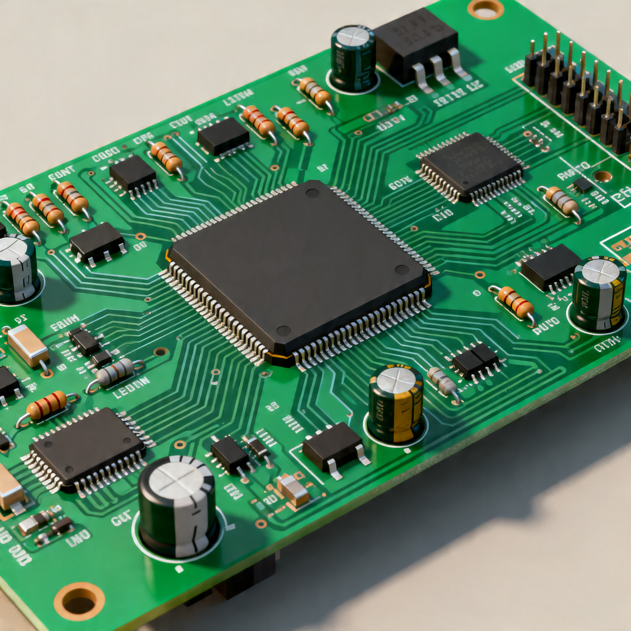
PCB assembly involves placing and soldering components onto a PCB to create a functional electronic circuit. High-volume SMT production requires precise coordination of design, fabrication, and assembly processes to ensure cost-effectiveness. Key concepts include understanding PCB design rules, optimizing layer stackup configurations, and selecting appropriate materials to maintain signal integrity. Adhering to industry standards, such as those provided by the IPC, ensures quality and reliability. By focusing on these core principles, manufacturers can achieve significant cost reductions while maintaining high production standards.
Detailed Specifications
Specifications are vital in PCB design and assembly, dictating how a board will perform and its manufacturing cost. Understanding and implementing the right specifications can lead to significant cost savings and improved product performance. The following tables provide detailed insights into PCB design rules, layer stackup options, and material properties.
| Design Rule | Minimum Value | Recommended Value |
|---|---|---|
| Trace Width | 0.1 mm | 0.15 mm |
| Trace Spacing | 0.1 mm | 0.15 mm |
| Via Diameter | 0.3 mm | 0.4 mm |
| Via Hole Size | 0.2 mm | 0.25 mm |
| Clearance to Edge | 0.5 mm | 1.0 mm |
| Pad Size | 0.5 mm | 0.7 mm |
| Solder Mask Clearance | 0.05 mm | 0.1 mm |
| Silkscreen Line Width | 0.1 mm | 0.15 mm |
| Aspect Ratio | 8:1 | 10:1 |
| Annular Ring | 0.1 mm | 0.15 mm |
Key Takeaways from the Specifications
The design rules outlined in the table are fundamental to achieving cost-effective PCB assembly. By adhering to the minimum and recommended values, manufacturers can ensure better electrical performance and manufacturability. For instance, maintaining appropriate trace widths and spacings minimizes the risk of short circuits and signal interference. Proper via sizing and aspect ratios enhance reliability and reduce the likelihood of manufacturing defects. These considerations not only reduce costs associated with rework and scrap but also improve overall product quality.
| Layer Configuration | Number of Layers | Application |
|---|---|---|
| Single Layer | 1 | Simple circuits, low-cost applications |
| Double Layer | 2 | Basic consumer electronics |
| Four Layer | 4 | Intermediate complexity, improved EMI |
| Six Layer | 6 | Advanced circuits, better signal integrity |
| Eight Layer | 8 | High-speed digital applications |
| Ten Layer | 10 | Complex, high-density designs |
| Twelve Layer | 12 | High-performance computing |
| Fourteen Layer | 14 | Military and aerospace applications |
Practical Implications
Choosing the right layer stackup configuration is crucial for balancing cost and performance. As the number of layers increases, so do the complexity and cost of manufacturing. However, higher layer counts offer better signal integrity and electromagnetic interference (EMI) control, essential for high-speed or sensitive applications. For instance, a four-layer board might suffice for consumer electronics, while a twelve-layer board is necessary for high-frequency communication devices. Understanding the trade-offs between cost and performance allows for informed decisions that can lead to significant cost savings without compromising functionality.
| Material | Dielectric Constant (Dk) | Loss Tangent (Df) |
|---|---|---|
| FR-4 | 4.5 | 0.02 |
| Rogers 4350B | 3.48 | 0.0037 |
| Rogers 4003C | 3.55 | 0.0027 |
| Isola FR408 | 3.75 | 0.009 |
| Arlon 85N | 3.5 | 0.004 |
| Nelco N4000-13 | 3.7 | 0.008 |
| Isola I-Tera MT40 | 3.45 | 0.0031 |
| Panasonic Megtron 6 | 3.5 | 0.002 |
| DuPont Pyralux | 3.2 | 0.0025 |
| Rogers TMM10i | 9.8 | 0.002 |
Application Guidelines
The choice of PCB material significantly impacts both the electrical performance and cost of the board. Materials like FR-4 are cost-effective for general applications but may not provide the necessary performance for high-frequency applications. Low-loss materials such as Rogers 4350B or Panasonic Megtron 6 are preferred for RF and microwave applications due to their low dielectric constants and loss tangents. Selecting the appropriate material based on the application's requirements ensures optimal performance and cost efficiency. Understanding these material properties helps in making informed decisions during the design phase, ultimately reducing unnecessary expenses.
Design Considerations
Effective PCB design requires attention to numerous factors to ensure cost efficiency and performance. First, adhering to design rules and specifications helps minimize manufacturing errors and defects. Employing design for manufacturability (DFM) principles ensures that the PCB can be produced efficiently without costly rework. Signal integrity is another crucial aspect, especially in high-speed designs; maintaining controlled impedance and reducing crosstalk are essential for reliable performance. Thermal management is also vital, as excessive heat can lead to component failure and reduced lifespan. Effective thermal vias, heat sinks, and proper component placement can mitigate these issues. Additionally, consider the use of automated design tools to optimize layout and reduce design time. By integrating these considerations into the design process, manufacturers can achieve a balance between cost and performance, leading to successful high-volume production.
Step-by-Step Implementation
Implementing cost reduction strategies in PCB assembly requires a systematic approach. Here are six detailed steps to follow:
- Design Optimization: Begin by optimizing the PCB layout for manufacturability. Use design automation tools to ensure adherence to design rules and minimize errors.
- Material Selection: Choose materials that provide the necessary performance at the lowest cost. Consider the application's requirements and select materials that offer the best balance of performance and cost.
- Layer Stackup Design: Determine the optimal layer stackup configuration based on the complexity and performance needs of the design. More layers may improve performance but increase cost, so balance is key.
- Manufacturing Collaboration: Work closely with your manufacturing partners to understand their capabilities and constraints. This collaboration can help identify cost-saving opportunities and avoid potential issues.
- Prototype Testing: Before full production, create prototypes to test design assumptions and identify any potential issues. This step allows for adjustments that can save costs in the long run.
- Continuous Improvement: After production begins, monitor performance and costs closely. Use this data to implement continuous improvement initiatives, further reducing costs over time.
Common Issues & Solutions
Even with careful planning, issues can arise during PCB assembly. Here are five common problems and their solutions:
- Problem: Solder bridging due to insufficient spacing. Solution: Adhere to recommended trace spacing and use solder mask to prevent bridging.
- Problem: Warping of the PCB. Solution: Use balanced layer stackups and proper material selection to reduce warping.
- Problem: Poor signal integrity. Solution: Implement controlled impedance traces and minimize crosstalk through careful layout.
- Problem: Component placement issues. Solution: Use automated placement tools and follow DFM guidelines to ensure correct component placement.
- Problem: Excessive heat generation. Solution: Implement effective thermal management strategies, such as heat sinks and thermal vias.
Applications & Use Cases
PCBs are used in a wide range of applications, from consumer electronics to industrial and aerospace systems. In high-volume production, cost-effective assembly is vital for consumer products like smartphones and tablets, where margins are thin and competition is fierce. In industrial applications, reliability and performance are paramount, necessitating robust designs with optimized signal integrity and thermal management. Aerospace and military applications require high-performance materials and complex layer stackups to meet stringent reliability standards. Understanding the specific requirements of each application helps in selecting the right design and assembly strategies to ensure success.
Selection & Sourcing Guide
Finding the right components and materials for PCB assembly is crucial for cost reduction. Use resources like IC Online to source components efficiently. Ensure that suppliers meet industry standards and provide reliable delivery schedules to avoid production delays. Establish strong relationships with suppliers to negotiate better pricing and terms.
FAQ
Here are some frequently asked questions about PCB assembly cost reduction:
- How can I reduce PCB assembly costs? Optimize design, select cost-effective materials, and collaborate with manufacturers.
- What is the importance of signal integrity? Signal integrity ensures reliable data transmission, crucial for high-speed applications.
- How do I choose the right PCB material? Consider the application's performance requirements and cost constraints.
- What are DFM principles? Design for manufacturability principles ensure that the PCB can be produced efficiently and cost-effectively.
- Why is thermal management important? Proper thermal management prevents component failure and extends the lifespan of the PCB.
- How do layer stackups affect cost? More layers increase cost but can improve performance; balance is key.
- What role do IPC standards play? IPC standards ensure quality and reliability in PCB design and manufacturing.
- How can prototype testing reduce costs? Testing prototypes helps identify issues early, allowing for adjustments before full production.
- What are some common PCB assembly issues? Issues include solder bridging, warping, and poor signal integrity, each with specific solutions.
- How can I ensure reliable component placement? Use automated placement tools and follow DFM guidelines.
Conclusion
Reducing PCB assembly costs in high-volume SMT production requires a comprehensive approach that includes optimized design, strategic material selection, and close collaboration with manufacturing partners. By adhering to industry standards and employing best practices, manufacturers can achieve significant cost savings while maintaining high-quality production. The strategies outlined in this article provide a roadmap for cost-effective PCB assembly, ensuring competitive advantage in the fast-paced electronics industry.