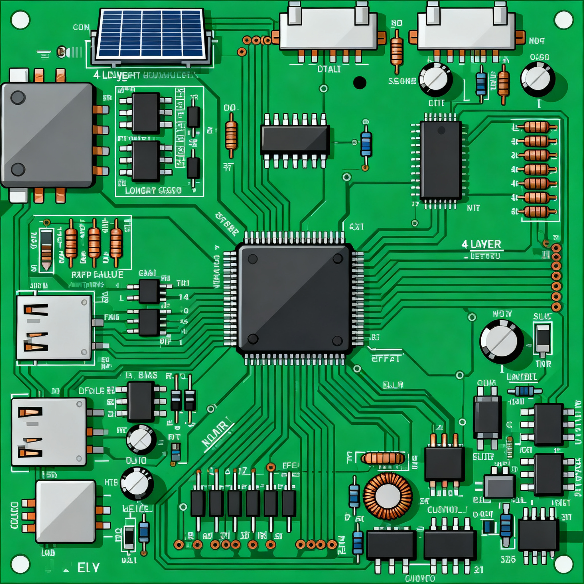
4-Layer Heavy Copper PCB Assemblies for Solar Inverter Control: A Practical Guide with Field Failure Analysis
When Salt, Moisture, and Thermal Stress Attack Solar Inverter PCBs: A Field Failure Reality Check You don’t have to look far to find solar inverter control boards that have failed long before their ra...
When Salt, Moisture, and Thermal Stress Attack Solar Inverter PCBs: A Field Failure Reality Check
You don’t have to look far to find solar inverter control boards that have failed long before their rated lifetime. I’ve walked through a photovoltaic power plant situated near an industrial zone where the air carried trace acidic gases. Inside the inverter cabinet, the first signs of trouble were obvious: dark, almost black rings around plated-through holes near the ventilation louvers. This was slow, relentless corrosion—sulfurous compounds and moisture working together to eat away the copper barrel walls. SprintPCB documented identical failure signatures, where acidic gas and humidity attack the hole walls and eventually create intermittent opens.
Field failures don’t stop at chemical corrosion. Moisture ingress combined with thermal cycling causes condensation inside the enclosure, which then wicks into micro-cracks in the solder mask or along the glass‑to‑resin interface of the laminate. Over time, the copper trace expands and contracts, and the sheer current density of a solar inverter’s power stage accelerates electro‑migration. Aivon points out that boards which haven’t been properly baked before assembly or which lose their conformal coating after a repair will fail quickly in the field, even if they passed initial bench tests.
Then there are the assembly‑related failures. Solder bridges, insufficient wetting on large component pads, and head‑in‑pillow defects on heavy copper footprints are far more common than many designers realize. AllPCB underscores that root‑cause analysis of these failures usually traces back to stencil design, reflow atmosphere, and the PCB surface finish. When you’re pushing 50 A or more through a single copper plane on a 4‑layer board, a marginal solder joint becomes a thermal fuse.
These real‑world failure modes make one thing clear: 4‑layer heavy copper PCB assemblies are no longer a specialty option for solar inverter control—they are the baseline for reliability. The combination of thick copper (≥3 oz) inner and outer layers, high‑Tg dielectrics, and carefully controlled fabrication processes is what keeps the board alive when salt, humidity, and thermal stress try to tear it apart.
How 4-Layer Heavy Copper Stacks Manage High Current and Thermal Cycling in Solar Inverters
A 4‑layer heavy copper board for a solar inverter doesn’t just carry current; it actively manages heat and mechanical stress. The stackup typically places the power planes on the inner layers (3–4 oz copper) and the high‑current routing on the outer layers (4–6 oz or more). This arrangement takes advantage of the larger cross‑section to reduce trace width, lower voltage drop, and spread heat away from hot spots. PCBonlie explains that the power architecture of a solar inverter—DC‑DC boost, full‑bridge, and gate drive—demands a board that can handle both continuous current and repetitive thermal cycling without delamination.
The dielectric material is just as important as the copper weight. High‑Tg FR‑4 with a glass transition temperature of at least 170 °C (and often 180 °C) is the workhorse. It resists softening during lead‑free assembly and maintains its mechanical properties when the board runs at 100 °C for hours each day. PCBMay notes that a 4‑layer heavy copper routing solution, built with high‑Tg FR‑4 and symmetrical copper distribution, has met continuous high‑efficiency power demands in commercial solar inverters. The symmetrical stack prevents warpage during reflow and ensures that the Z‑axis expansion is uniform across the board.
Current density and thermal resistance are managed by the interplay of copper thickness and trace geometry. A 4‑layer design allows you to route high‑current paths on multiple layers and stitch them with an array of vias, effectively creating a parallel conductor that reduces both DC resistance and AC losses. EBest PCB emphasizes that heavy copper is useful only when the geometry can be fabricated and assembled; the fabricator must be capable of etching fine spaces between thick copper traces and plating the hole walls uniformly.
Table 1: 2‑Layer vs. 4‑Layer Heavy Copper PCB Characteristics for Solar Inverter Control
| Parameter | 2‑Layer Heavy Copper (≥3 oz) | 4‑Layer Heavy Copper (Inner ≥3 oz, Outer ≥4 oz) | Selection Note |
|---|---|---|---|
| Current carrying capacity | Limited to one or two high‑current paths; must use wide traces | Multiple parallel paths on inner and outer layers with via stitching; supports 50 A+ continuous | 4‑layer is mandatory for multi‑phase inverter stages |
| Thermal dissipation | Relies on outer copper planes; limited heat spreading | Inner copper planes act as heat spreaders; lower thermal resistance to ambient | 4‑layer reduces hotspot temperature by 10–15 °C in typical designs |
| Impedance control for gate drives | Difficult to maintain controlled impedance with thick copper on a single reference plane | Dedicated inner ground plane enables clean return paths and controlled impedance for high‑speed gate signals | Critical for SiC and GaN switching circuits |
| EMI shielding | Poor shielding; high‑current loops radiate | Inner power/ground plane pair provides natural shielding; reduces radiated emissions | 4‑layer helps meet CISPR 11 without extra shielding cans |
| Warpage during reflow | Asymmetrical copper distribution risks warpage | Symmetrical stackup (e.g., 4 oz/3 oz/3 oz/4 oz) minimizes warpage | Symmetry is a must for lead‑free reflow |
| Fabrication complexity | Lower; fewer layers to bond | Higher; requires controlled lamination and uniform plating of high‑aspect‑ratio holes | Only work with fabricators that have heavy copper DFM capability |
The jump from 2 to 4 layers in heavy copper is not just about more routing space. It’s about creating a robust thermal‑electrical‑mechanical system. The inner planes act as a low‑impedance return path for switching currents, which reduces ground bounce and improves the reliability of the control circuitry. The symmetrical stackup distributes mechanical stress evenly, so the board survives hundreds of thermal cycles from –40 °C to +125 °C without barrel cracking.
4-Layer Heavy Copper FR-4 vs. MCPCB for Solar Inverters: When to Choose Each
Metal‑core PCBs (MCPCBs) have long been the go‑to for high‑power LED applications, and they sometimes appear in solar inverter designs. But the assumption that MCPCBs are always superior for thermal management can lead to costly, hard‑to‑repair assemblies. AllPCB notes that MCPCBs are more expensive than FR‑4, and their single‑layer or sometimes double‑layer structure severely limits routing density. For a solar inverter control board that combines power paths, gate drivers, and a microcontroller, that single‑layer limitation is a dealbreaker.
4‑layer heavy copper FR‑4 stacks, when designed with high‑Tg materials and adequate copper, can rival MCPCBs in thermal performance for many inverter sections. HilPCB highlights that high‑Tg PCBs with adhesion‑optimized heavy copper foils provide better thermal stability and reduce delamination risk under sustained heat. The key advantage of FR‑4 is the ability to route multiple layers, which is essential for the mixed‑signal nature of an inverter control board. EBest PCB reinforces that material selection must follow voltage stress, temperature, and current density, and that heavy copper is useful only when the geometry can be fabricated and assembled—a condition that FR‑4 stacks readily meet with the right fabricator.
Repairability is another critical differentiator. An MCPCB is notoriously difficult to rework. If a power transistor fails in the field, heating the metal base to remove the component often damages the thin dielectric layer. FR‑4 heavy copper boards allow standard rework with hot air and pre‑heating plates, and the component can be replaced without compromising the board. PCBMay demonstrated a commercial 4‑layer heavy copper routing solution that met continuous high‑efficiency power execution demands, proving that FR‑4 can handle the thermal load when designed correctly.
Table 2: 4‑Layer Heavy Copper FR‑4 vs. MCPCB for Solar Inverter Applications
| Metric | 4‑Layer Heavy Copper FR‑4 (High‑Tg) | MCPCB (Aluminum Base) | Selection Criteria & Failure Boundary |
|---|---|---|---|
| Thermal conductivity (through‑plane) | 0.3–0.4 W/m·K for FR‑4 dielectric; heat carried by copper planes | 1.0–3.0 W/m·K for dielectric layer; metal base spreads heat | MCPCB wins for concentrated hotspots; FR‑4 needs copper area |
| Cost (relative) | 1.0× (baseline) | 1.5×–2.5× | FR‑4 is more cost‑effective for 4‑layer and above |
| Routing layers | 4 (or more) with via stitching | Typically 1 or 2 layers | FR‑4 required for mixed‑signal control & power routing |
| Repairability | Excellent; standard rework tools | Poor; risk of dielectric damage during rework | FR‑4 is preferred for field‑serviceable inverters |
| Power density capability | High; multiple copper layers handle high current | Moderate; limited by trace width on a single layer | FR‑4 supports higher power density with proper design |
| Dielectric insulation integrity | High‑Tg FR‑4 with CTI ≥ 175 V; tested for high‑voltage clearance | Thin dielectric layer (≈0.1 mm) may break down under high‑voltage transients | FR‑4 offers better insulation for 600 V–1500 V systems |
MCPCBs still have a place in solar inverters—typically for the boost inductor or a dedicated power module that requires the lowest possible thermal resistance. But for the main control board that integrates the DSP, gate drivers, and high‑current paths, 4‑layer heavy copper FR‑4 is the pragmatic choice. It gives you the routing density, insulation integrity, and repairability that solar field service demands, without the cost penalty of a metal core. A thermal simulation during the design phase will confirm whether the FR‑4 stack can keep junction temperatures in check; in most cases it can, provided the copper area is sufficient.
Design Rules and DFM Checks That Prevent Field Failures in 4-Layer Heavy Copper Solar Inverter Boards
Preventing the field failures we saw earlier—corrosion, solder defects, insulation breakdown—starts with design rules that are specific to heavy copper and high‑voltage solar environments. EBest PCB stresses that you must verify the complete insulation path: calculate clearance and creepage from the working voltage, transients, material group, pollution degree, altitude, and insulation type. A component package with a stated isolation rating doesn’t guarantee the board‑level insulation if the PCB layout ignores creepage across slots or exposed copper.
Solder defects are a dominant failure mode on heavy copper pads. AllPCB details that stencil design, reflow atmosphere, and component coplanarity are the usual suspects. For a 4‑layer board with 4 oz outer copper, the thermal mass of the pads is enormous. You need a stepped stencil or a thicker deposit to ensure enough solder volume, and the reflow profile must be extended to allow the entire pad to reach peak temperature without overheating smaller components.
Environmental protection is non‑negotiable. Aivon recommends applying fresh conformal coating post‑repair and baking boards pre‑assembly if there is any suspicion of moisture. But coating alone won’t save a board that has insufficient copper wall thickness in the vias. The dark rings around vias that SprintPCB documented are a direct result of corrosive gases penetrating the barrel wall. The countermeasure is to specify a minimum copper wall thickness of 25 µm (or more) after plating, and to avoid routing sensitive vias directly next to enclosure vents.
Table 3: DFM Parameters for 4‑Layer Heavy Copper Solar Inverter Boards
| Parameter | Recommended Value/Range | Impact on Field Failure |
|---|---|---|
| Outer copper weight | 4 oz – 6 oz | Insufficient weight leads to trace overheating and thermal runaway |
| Inner copper weight | 3 oz – 4 oz | Lower weight reduces current sharing and increases hot spots |
| Minimum trace/spacing (outer) | 10 mil / 10 mil for 4 oz; wider for 6 oz | Violations cause etching shorts, reduced creepage, and field corrosion |
| Drill‑to‑copper clearance | ≥ 12 mil for inner layers | Insufficient clearance risks CAF (conductive anodic filament) growth under humidity |
| Dielectric thickness (prepreg) | ≥ 5 mil after lamination | Thinner dielectrics compromise high‑voltage insulation and increase capacitive coupling |
| Base material CTI | ≥ 175 V (PLC 3) or higher | Low CTI leads to tracking and surface flashover under polluted conditions |
| Copper wall thickness in vias | ≥ 25 µm (1 mil) | Thinner walls are more susceptible to corrosion and thermal cycling fatigue |
| Conformal coating thickness | 50 µm – 100 µm | Thin coating fails to block acid gases; thick coating may crack under thermal stress |
Here are the actionable design and assembly steps that will keep your 4‑layer heavy copper solar inverter board reliable:
- Start with a DFM review from your fabricator. EBest PCB recommends requiring a DFM response against the proposed layer count, copper weight, dielectric construction, hole structure, and high‑voltage features. This report will flag any spacing or drilling limitations before you commit to production.
- Optimize the stencil for heavy copper. Use a stepped stencil with a thicker deposit (e.g., 8–10 mil) on high‑current pads. Electro‑formed or laser‑cut stencils with rounded apertures improve paste release and reduce bridging on fine‑pitch components.
- Bake the boards before assembly. Moisture trapped in the laminate can cause delamination during reflow. A 4‑hour bake at 125 °C is a cheap insurance policy, especially for boards stored in humid environments.
- Verify the complete insulation path. Check creepage and clearance at every point: between component leads, across cutouts, under fasteners, and at the coating boundary. An isolation symbol on the silkscreen is not enough.
- Apply conformal coating after assembly and after any repair. Even a small repair that removes coating can create a corrosion pathway. Aivon’s advice to reapply coating post‑repair is a standard practice that must be enforced in the field.
- Use thermal simulation to validate the stackup. PCBonlie provides reliability engineering insights that help you predict junction temperatures and identify hot spots before the first prototype is built.
Tip: When you engage with a PCB assembly partner like NovaPCBA, ask for their heavy copper process capability data—including minimum trace/spacing for 4 oz and 6 oz copper, drill registration accuracy, and their experience with high‑voltage solar inverter boards. This upfront alignment prevents fabrication surprises and field failures down the road.
4-Layer Heavy Copper Solar Inverter PCB FAQ: What Senior Engineers and Buyers Ask
Q: What copper weight is typically used for 4‑layer solar inverter control boards?
Inner layers often use 3–4 oz copper, while outer layers can go up to 6 oz or more, depending on current density. The exact stackup is determined by the required ampacity and thermal management, not a fixed rule. For a 20 kW inverter, a common stackup is 4 oz outer / 3 oz inner / 3 oz inner / 4 oz outer. Simulation of trace temperature rise under full load is the final arbiter.
Q: How do you verify insulation integrity after heavy copper lamination?
Creepage and clearance distances must be recalculated for the actual working voltage, pollution degree, and material group. High‑pot testing (typically 2× rated voltage + 1000 V for one minute) and partial discharge inspection on the assembled board validate the insulation path, especially near slots and exposed copper. The board must pass these tests both before and after conformal coating.
Q: Which surface finish is best for high‑current heavy copper pads?
ENIG (electroless nickel immersion gold) is common for corrosion resistance and flatness, but for heavy copper, HASL with lead‑free alloy or immersion silver can be used if the finish can withstand multiple thermal cycles. The choice must also consider shelf life and assembly process compatibility. Silver can tarnish, so it needs careful handling; ENIG avoids that but can suffer from black pad if not controlled. Many successful solar inverter designs use ENIG with a nickel thickness of 3–5 µm.
Q: Can a 4‑layer heavy copper FR‑4 board replace an MCPCB for cost savings?
Yes, in many solar inverter control sections where the heat load is moderate and the board area is sufficient. 4‑layer heavy copper FR‑4 provides better routing density and repairability, while MCPCBs are harder to rework and more expensive, as noted by AllPCB. Thermal simulation should guide the decision; if the component junction temperature stays within derated limits, FR‑4 is the cost‑effective choice.
Q: What are the early warning signs of field corrosion in plated‑through holes?
Dark rings around via holes near housing vents, intermittent open circuits under thermal cycling, and increased via resistance. These signs, documented by SprintPCB, indicate acidic gas and moisture attack and call for immediate conformal coating reapplication and possibly a board redesign with heavier copper wall thickness. If you measure via resistance during a post‑mortem and find it has increased by more than 10%, the barrel is corroding.
Q: How do I specify DFM feedback for a 4‑layer heavy copper stack‑up?
Request a full DFM report covering copper weight capability, minimum trace/spacing for heavy copper, drill‑to‑copper clearance, dielectric thickness, and laminate material group. EBest PCB recommends requiring a DFM response against the proposed layer count, copper weight, dielectric construction, and high‑voltage features to avoid fabrication surprises. The report should highlight any potential for under‑etching, over‑plating, or layer misregistration that could compromise insulation or current capacity.
Conclusion
The shift to 4‑layer heavy copper PCB assemblies for solar inverter control isn’t a trend—it’s a direct response to the physical realities of high‑current switching, thermal cycling, and corrosive environments. When you see dark rings around vias on a failed board, that’s the cost of ignoring copper thickness and conformal coating. By choosing the right stackup, running DFM checks, and comparing FR‑4 heavy copper with MCPCBs based on actual thermal data, you can build a board that lasts 15 years in the field. At NovaPCBA, we routinely assemble 4‑layer heavy copper boards for solar inverter manufacturers, handling everything from high‑Tg material selection to precision stencil printing and conformal coating application. Our DFM reviews catch the insulation and spacing issues that lead to field failures, so your next inverter control board doesn’t become another corrosion case study.
References & Further Reading
- SprintPCB – Solar Inverter PCB: Building Long‑Term Reliability Against Salt, Moisture, and Thermal Stress
- Aivon – Troubleshooting Common Issues in Solar Inverter PCBs: A Practical Approach
- EBest PCB – Solar Inverter PCB Assembly
- AllPCB – Solar Inverter PCB Assembly: A Step by Step Guide for Manufacturers
- AllPCB – Advanced PCB Materials for Solar Inverters: Enhancing Performance and Durability
- HilPCB – Solar Inverter PCB Manufacturing and Quality Control
- PCBMay – Solar Inverter PCB Manufacturer | High‑Voltage PV PCBA
- PCBonlie – Solar Inverter Circuit Boards: Design, Engineering & Implementation