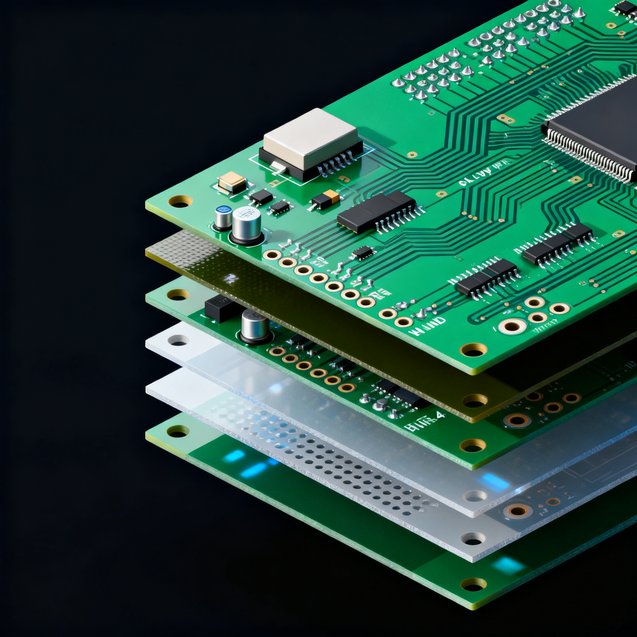
2026 Manufacturing Best Practices for 6-Layer PCB Stack-Up Design: Impedance Control, Via Types, and Material Selection
Why Six Layers? The Signal Integrity and Density Tipping Point Most engineers start with a 4‑layer board and immediately run into two walls: routing congestion under a dense BGA, and the impossibility...
Why Six Layers? The Signal Integrity and Density Tipping Point
Most engineers start with a 4‑layer board and immediately run into two walls: routing congestion under a dense BGA, and the impossibility of holding tight impedance targets when reference planes are shared or absent. Moving to six layers doesn’t just add two copper planes—it re‑organizes how signals, power, and ground relate to one another. As one design guide notes, the real advantage is the ability to organize signals, references, and power so routing density improves without sacrificing return‑current integrity. When you’re driving DDR4, PCIe Gen4, or multiple MIPI lanes, that reorganization becomes a signal‑integrity prerequisite, not a luxury.
But the wrong stack‑up creates problems worse than a crowded 4‑layer board. Return currents in high‑speed signals follow the path of lowest inductance, not the schematic’s DC path. If L3 and L4 are stuffed with high‑speed traces and neither is adjacent to a solid reference plane, the return current is forced to wander, coupling into unrelated nets and radiating. Return currents in high‑speed signals will follow the path of lowest impedance, and a missing adjacent plane stretches that path, raising loop inductance and causing signal distortion or increased EMI. The result: a 6‑layer board that radiates worse than a properly designed 4‑layer board.
In 2026, component pitches of 0.4 mm and edge rates below 30 ps make a haphazard stack‑up a manufacturing risk. PCB fabricators are rejecting more designs at CAM because trace widths dictated by impedance targets fall below etch capabilities, or because prepreg thicknesses can’t meet the specified dielectric spacing. The decision to go to six layers must be paired with stack‑up discipline from the very first footprint placement. Below we break down the manufacturing best practices that separate a first‑pass success from a three‑week engineering change spiral.
How a Stack‑Up Dictates Impedance—and Why Your Fab Drawing Needs It
Impedance control isn’t a button you check at the end of layout; it’s a stack‑up geometry exercise that happens before routing. Single‑ended 50 Ω and differential 100 Ω targets are the lingua franca of high‑speed design, but the trace width that hits 50 Ω on Layer 1 depends on the dielectric thickness between L1 and L2, the copper weight, and the Dk of the prepreg. A standard 1.6 mm FR4 board with 1 oz outer copper and 0.5 oz inner copper offers a well‑characterized baseline. One fabrication reference shows that for a typical 4.2 Dk and a 3.5‑mil prepreg thickness between L1 and L2, a 5.5‑mil trace hits roughly 50 Ω, while a 100 Ω differential pair sits around 4.5‑mil width with 7‑mil spacing. Those numbers shift dramatically if you specify 2 oz outer copper or if the fabricator substitutes a different prepreg to meet a total thickness target.
The takeaway for 2026: your Gerber package must include an explicit impedance table and a stack‑up drawing that calls out material types, copper weights, and layer‑to‑layer dielectric thicknesses. Fabricators increasingly use TDR testing to verify impedance on impedance‑controlled orders, and without a table they’ll default to generic values that may not match your simulation. For impedance‑controlled designs, TDR testing verifies impedance values alongside flying‑probe or fixture testing that confirms continuity and isolation before any components are placed. That dual verification catches opens, shorts, and impedance excursions before they turn into field failures.
Board thickness itself is a manufacturing variable that engineers overlook. Most 6‑layer designs target 1.6 mm (0.062 inches) because it’s the sweet spot for connector fit, mechanical stiffness, and standard laminate availability. A 6‑layer PCB thickness of 1.6 mm is the most common reference point in fabricator capability sheets, but 0.8, 1.0, 1.2, and 2.0 mm variants appear in wearables, mezzanine cards, and backplanes. Each alternative reduces the dielectric window, forcing tighter trace geometries that can violate minimum etch rules. When a design calls for a 0.8 mm total stack‑up, the fabricator often has to thin the core to an extent that the inner traces become too narrow—a leading cause of CAM rejection.
| Parameter | Typical Value (Standard 6‑layer, 1.6 mm) | Unit/Notes |
|---|---|---|
| Total thickness | 1.60 ± 0.16 | mm; 0.8, 1.0, 1.2, 2.0 mm options available |
| Outer copper weight | 1 oz (35 µm) | Start with plating; 0.5 oz possible on inner layers |
| Inner copper weight | 0.5 oz (18 µm) | Often with lower etch capability (3.5–4 mil min trace/space) |
| Prepreg thickness L1–L2 / L5–L6 | 3.0–4.0 mil (76–102 µm) | Adjusted based on target impedance |
| Core thickness L2–L3 / L4–L5 | 8–12 mil (203–305 µm) | Separates signal layers from power planes |
| Dielectric constant (FR4, typical) | 4.2–4.5 at 1 GHz | Varies with resin content; mid‑loss materials Dk 3.8–4.0 |
| Single‑ended impedance target | 50 Ω ±10% | USB, HDMI, DDR address/command |
| Differential impedance target | 100 Ω ±10% | PCIe, USB 3.x, LVDS |
| Min trace width for 50 Ω on L1 | ~5.5 mil (4.2 Dk, 3.5‑mil prepreg) | Recalculate for each layer pair |
| TDR test requirement | Yes, with coupon | Fabricator adds test coupon on panel edge |
| Electrical test method | Flying probe or fixture, ±50 V | Verifies continuity, isolation; TDR optional surcharge |
These numbers are not fixed—they come alive when the fabricator adjusts weave style, resin content, and pressing conditions. That’s why locking the stack‑up before layout is essential. Share your target impedance values with the fab house during pre‑CAM review, and ask for a recommended dielectric stack. This single step prevents the iterative “your trace is too narrow for our process” email that can add a week to prototyping.
Stack‑Up Configurations Compared: When Route, Power, and Ground Planes Collide
Choosing a 6‑layer stack‑up is a three‑way negotiation between signal‑return quality, power distribution, and routing density. Four practical configurations dominate production designs in 2026, each with a distinct failure boundary.
Configuration A: Signal‑GND‑Signal‑Signal‑GND‑Signal (no dedicated power plane) is the simplest structure. It puts two solid ground planes at L2 and L5, giving L1 and L6 a clean return path. But L3 and L4 are left without an adjacent reference. Leaving L3 and L4 without adjacent reference planes forces longer return paths and risks radiation. Power is distributed as a routed net on signal layers, which works for low‑current, low‑speed designs but breaks down with multiple voltage rails above 500 mA.
Configuration B: Signal‑GND‑Signal‑Power‑GND‑Signal adds a dedicated power plane on L4, sandwiched between GND on L5 and Signal on L3. This arrangement gives signals on L3 a nearby reference (power or ground), while L4‑L5 form a close‑coupled power‑ground pair that provides excellent decoupling at high frequencies. Wonderful PCB’s standard stack‑up highlights this as preferred for multi‑voltage designs because the power plane adjacency to both L3 and GND improves plane capacitance. The cost is one lost signal layer—you’re down to four routing layers plus power.
Configuration C: Signal‑GND‑Signal‑GND‑Power‑Signal takes EMI performance a step further. With two ground planes (L2 and L4), differential pairs on L1 and L3 have a ground reference immediately beneath them, creating the tight loop area that minimizes radiated emissions. The dual‑ground‑plane layout creates optimal conditions for high‑speed differential pairs and controlled impedance but leaves only three routing layers. It’s the go‑to choice for USB 3.2, HDMI 2.1, and PCIe Gen4 designs where signal fidelity trumps routing density.
Configuration D: Hybrid RF/digital stack‑up (Signal‑GND‑Signal‑Power‑Signal‑GND or similar) separates sensitive analog or RF sections onto outer layers with buried stripline routing inside. This custom approach often combines Rogers or ISOLA low‑loss material on specific layers with standard FR4 cores, and is driven by the RF front‑end rather than the digital section. Manufacturing cost rises sharply because of mixed material lamination cycles.
| Comparison Metric | Config A (Signal‑GND‑Signal‑Signal‑GND‑Signal) | Config B (Signal‑GND‑Signal‑Power‑GND‑Signal) | Config C (Signal‑GND‑Signal‑GND‑Power‑Signal) | Selection Criteria & Failure Boundary |
|---|---|---|---|---|
| Dedicated power plane | No | Yes, on L4 | Yes, on L5 | Config A fails with >2 voltage rails or >500 mA; Config B/C support PDN design. |
| Ground planes | 2 (L2, L5) | 2 (L2, L5) | 2 (L2, L4) | Config C provides <0.1 mm L1‑GND spacing, best for 10 GHz+ EMI control. |
| Routing layers | 4 signal layers | 3 signal layers + power plane | 3 signal layers | Config A best for dense digital w/o power integrity constraints; Config C sacrifices one routing layer. |
| Typical impedance target feasibility | 90 Ω diff on L1/L6 easy; L3/L4 uncontrolled | 50 Ω/100 Ω on L1/L6 and L3, L4‑L5 tight coupling | 50 Ω/100 Ω on L1/L3 and L6; superb isolation | Config B is the workhorse; Config C if EMI compliance is tight (CISPR 32 Class B). |
| Crosstalk risk | High on L3‑L4 (no reference plane) | Moderate; L3 adjacent to PWR | Low; all signal layers have immediate GND reference | Do not route high‑speed on L3/L4 in Config A. |
| Relative cost vs 4‑layer | +30‑40% | +35‑50% | +45‑65% | PCBark quantifies a 30–65% premium over a 4‑layer board; Config C at upper end. |
| Lead time impact | Standard 5‑7 days | Standard | May add 1‑2 days for TDR coupon verification | Rushed 48‑hour turn doubles cost per PCBSync. |
| Controlled impedance surcharge | Optional; +0‑10% if limited traces | Typical +8‑15% | Typical +15‑20% | Specifying controlled impedance can add 3 weeks lead time as a medical device case study illustrates; design review needed. |
Choosing between B and C often comes down to your compliance margin. If conducted emissions are already borderline on a 4‑layer prototype, Config C’s dual‑ground arrangement can pull you back within limits without resorting to shield cans. But if you need five separate power rails for an FPGA and its I/O banks, Config B gives you a solid power plane without starving routing space. In 2026, many fabricators keep pre‑approved stack‑up libraries for Config B at 1.6 mm thickness—using one of those libraries eliminates the NRE for a custom stack‑up and reduces lead time by at least a week.
Via Selection, Material Grades, and Three Cost Traps Designers Walk Into
Via strategy on a 6‑layer board isn’t a post‑route tidy‑up; it determines whether high‑speed signals launch cleanly or radiate at every layer transition. Through‑hole vias remain the cost anchor, but at data rates above 10 Gbps the unused via stub creates a resonant dip that saps eye height. A buried via from L2 to L5 excises the stub, turning a resonant structure into a clean transition. The penalty: a sequential lamination cycle that adds at least one extra pressing and drilling step. At NovaPCBA, we often see designers blindly select blind vias for all BGA escapes without considering that a 0.8‑mm pitch BGA on a 1.6‑mm board can be fully escaped with through‑hole vias and two routing layers if the stack‑up is planned early.
Material selection follows a similar frugal logic. High‑Tg FR4 (Tg150–170) covers the vast majority of 6‑layer boards operating below 8 GHz because its thermal stability prevents barrel cracking during reflow and its dielectric properties are well‑characterized. Weller’s reference designs emphasize Tg150 as sufficient for mainstream 6‑layer stack‑ups before jumping to exotic laminates. The trap is specifying Megtron 6 or Rogers 4350 “just to be safe” on a board where the longest PCIe Gen4 channel is 5 inches. That choice roughly doubles the material cost and forces the fabricator to order a specialty laminate lot, adding two weeks to procurement.
Three cost traps recur in 6‑layer projects every quarter:
- Non‑standard thickness that forces a custom stack‑up. Every deviation from 1.6 mm, 1.2 mm, or 0.8 mm requires a fresh dielectric calculation and a one‑off pressing program. The NRE and material surcharge can add 20–30% to a prototype run. Check your mechanical enclosure before locking the thickness.
- Unnecessary controlled‑impedance call‑outs on short links. A USB 3.2 trace under 40 mm with a clean reference plane often meets the eye‑diagram mask without a formal TDR‑verified impedance spec. A 2024 medical device design carried USB 3.2 Gen1 at 5 Gbps on traces under 40 mm and skipped the full controlled‑impedance specification, saving 38% on fab cost and avoiding a 3‑week lead‑time stretch. The key is to simulate the channel and decide based on margin, not fear.
- Ignoring the fabricator’s standard stack‑up library. Every established fabricator has pre‑qualified 6‑layer stack‑ups with known impedances. Starting from one of those and adjusting only what’s necessary eliminates the back‑and‑forth CAM queries that delay release by 24–48 hours. Ask for the library during vendor selection.
Manufacturing best practices that prevent field failures extend beyond the bare board. During assembly, panel fiducials, silkscreen legibility for polarity markings, and flying‑probe testing for continuity and isolation are the last line of defense. This assembly guide underscores that flying‑probe testing catches opens and shorts before components are placed, while AOI confirms solder fillet quality. Together, these steps ensure that a perfectly fabricated 6‑layer board doesn’t fail because of a reversed capacitor or a missed solder joint.
| Parameter | Through‑Hole Via | Blind Via (L1‑L3) | Buried Via (L2‑L5) | Material Grade | Relative Raw Material Cost |
|---|---|---|---|---|---|
| Typical use case | BGAs >0.5 mm pitch, all non‑critical signals | Escape 0.4 mm pitch BGA; dense routing | Remove stub on 10 Gbps+ pairs; via‑in‑pad | Standard FR4 (Tg 130‑140) | 1x |
| Stub impact | Resonant dip above 5‑8 GHz depending on length | Stub reduced (L1 entry, L3 exit) | No stub; nearly transparent to 28 Gbps | High‑Tg FR4 (Tg 150‑170) | 1.05–1.15x |
| Fabrication complexity | Single lamination, standard drill | Sequential lamination + controlled depth drill | Sequential lamination + two drill cycles | Mid‑loss (e.g., ISOLA 370HR, Dk 3.9) | 1.3–1.6x |
| Cost adder vs through‑hole | Baseline | +20‑30% | +35‑50% | Low‑loss (Megtron 6, Rogers 4350B) | 1.8–2.5x |
| Lead time impact | Standard 5‑7 days | +3‑5 days | +5‑8 days | Specialty low‑loss materials add 1‑2 weeks procurement | — |
The art of 6‑layer design in 2026 is to pick the minimum viable via technology that meets signal integrity requirements while staying within standard processing. Before releasing a Gerber package, run this checklist:
- Impedance table: List each controlled trace class (50 Ω SE, 90 Ω, 100 Ω diff), the layer pair, target tolerance (±10% typical), and the geometric trace width/space you used. Add a note if TDR testing is required.
- Stack‑up drawing: Show every layer with material call‑out (e.g., “Prepreg 2116, 62% resin”), copper weight, and finished dielectric thickness. Mark the layer order and total thickness.
- Via definitions: Specify which vias are through‑hole, blind, buried, or back‑drilled. Include start/stop layers and drill size. Note if via‑in‑pad plugging is required.
- Material specification: State Tg, Dk at 1 GHz, and any IPC‑slash sheet (e.g., IPC‑4101/126 for lead‑free compatible). If mixing materials, define each region clearly.
- Test requirements: Indicate continuity/isolation test (standard), TDR coupon for specific nets, and any AOI or x‑ray inspection for BGAs after assembly.
When you hand this package to NovaPCBA’s pre‑CAM team, the stack‑up goes into a familiar simulation environment, and the fabricator can flag conflicts before copper is poured. That front‑loaded communication prevents the 80% of re‑spins that originate from a missing dielectric thickness or an over‑constrained impedance spec.
Pre‑CAM Questions Engineers Ask Before Sending a 6‑Layer Impedance‑Controlled Board
Q: Our 6‑layer board has USB 3.0 traces under 40 mm. Do we really need controlled impedance, or can we save cost and lead time?
For short traces with clean, continuous reference planes, many fabricators can hold adequate impedance without the formal controlled‑impedance surcharge and associated TDR documentation. One medical device design carried 5 Gbps USB 3.2 Gen1 on traces under 40 mm and skipped the full TDR spec, reducing fab cost by 38% and avoiding a 3‑week lead‑time stretch. The caveat: this works only if your stack‑up is a standard configuration (e.g., Config B at 1.6 mm) and the trace geometry stays within the fabricator’s normal process window. If your simulation shows less than 2 dB margin at 2.5 GHz, add the controlled‑impedance flag for safety.
Q: What is the most common 6‑layer stack‑up that balances cost, routability, and signal integrity?
The Signal‑GND‑Signal‑Power‑GND‑Signal arrangement with a dedicated power plane on L4 (or L3) is the industry workhorse. It gives two solid reference planes—L2 and L5—for signals on L1/L3 and L4/L6, supports multiple voltage rails through the power plane, and uses standard 1.6 mm thickness that every large‑volume fabricator can produce without NRE surcharge. Deviating from this configuration—by shifting to a dual‑ground‑plane stack or eliminating the power plane—raises cost more than any other single choice, because it forces a custom lamination cycle.
Q: How do I choose between blind vias and through‑hole vias on a 6‑layer board?
Through‑hole vias are sufficient unless you must escape 0.4 mm pitch BGAs or route PCIe Gen4/5 differential pairs that cannot tolerate a via stub. Blind vias add approximately 20–30% to fabrication cost due to sequential lamination and controlled‑depth drilling. A buried via from L2 to L5—used to eliminate stubs on critical differential pairs—requires two sequential lamination steps and adds at least a week to lead time. Reserve blind/buried technology for the nets where an electrical simulation shows a failing eye diagram with a conventional through‑hole via.
Q: Why do some fabricators reject my 6‑layer stack‑up with 0.5 oz inner copper when I ask for 100 Ω differential impedance?
A 100 Ω differential target on thin inner cores often forces trace widths below the fabricator’s minimum etch capability—typically 3.5 mil for 0.5 oz copper. When the required width drops to 3.0 mil to meet the impedance goal, the fabricator cannot reliably pattern those traces. The solution is to provide a tolerance band (e.g., ±10% impedance) and allow the fabrication house to adjust core thickness or copper weight. An alternative is to route the differential pair on an outer layer where 1 oz copper offers more room for etch compensation, or to use a slightly higher Dk prepreg to widen the trace geometry.
Q: Is high‑Tg FR4 enough, or should I specify a low‑loss laminate for a 6‑layer board with PCIe Gen4?
High‑Tg FR4 (Tg150–170) works for most PCIe Gen4 channels below 10 inches if the stack‑up is well‑optimized and differential spacing is tight. When traces exceed that length or the board operates continuously above 8 GHz, a low‑loss material such as Megtron 6 or Rogers 4350B is advisable, but it roughly doubles the raw material cost and may require a specialized press cycle. Before specifying an exotic laminate, simulate the channel loss at 8 GHz using the actual stack‑up geometry and decide based on eye‑opening margin, not a blanket datasheet Df number.
Summary and next steps. The jump to six layers is a strategic inflection point: it solves density and signal‑integrity bottlenecks but only if the stack‑up, via architecture, and material grade are aligned from day one. A well‑documented impedance table, a fabricator‑friendly stack‑up drawing, and a clear decision on via technology cut the number of design spins in half. For engineering teams that want to off‑load the CAM negotiation and assembly integration, NovaPCBA offers full turnkey service from bare‑board fabrication to component procurement and final assembly—handling 6‑layer controlled‑impedance boards at competitive lead times. By baking manufacturing constraints into the stack‑up before routing starts, you turn a prototype gamble into a predictable production ramp.
References & Further Reading
- 6 Layer PCB Assembly Demystified: Best Practices for Reliable Manufacturing – AllPCB
- Ultimate Guide to 6 Layer PCB Stackup Design & Manufacturing – ELEPCB
- 6 Layers PCB Manufacturing: Advanced Stack‑up, Design Guidelines, and Cost Analysis – Wonderful PCB
- 6‑Layer PCB Stackup: Design Guide for Real‑World Manufacturing – PCBCool
- 6 Layer PCB Board Manufacturing – Wonderful PCB
- 6‑Layer PCB Stackup Design: Complete Guidelines for Optimal Performance – WELLER
- 6 Layer PCB Design Guide: Stackup, Impedance & Vias (2026) – PCBark
- 6‑Layer PCB Stackup: Layer Order,