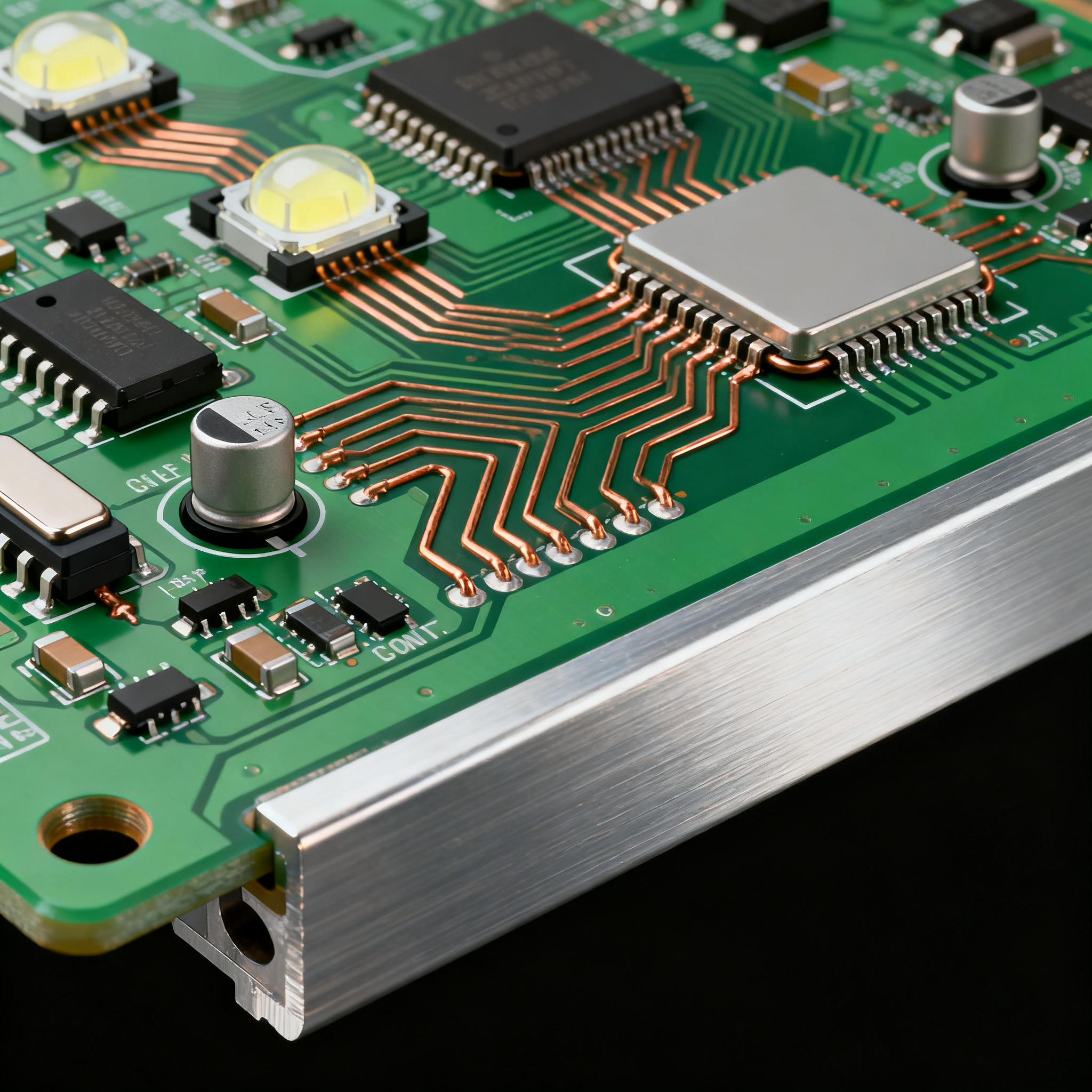
2026 Best Practices for High-Reliability Aluminum Core PCB Assembly in LED Lighting Systems
The Thermal Reality Check: Why Aluminum Core PCB Assembly Is No Longer Optional for High-Power LED Systems LED efficacy now routinely exceeds 180 lm/W, and compact chip‑on‑board modules pack 50 W to 3...
The Thermal Reality Check: Why Aluminum Core PCB Assembly Is No Longer Optional for High-Power LED Systems
LED efficacy now routinely exceeds 180 lm/W, and compact chip‑on‑board modules pack 50 W to 300 W into footprints smaller than a business card. That progress has pushed conventional FR‑4 substrates well past their thermal limits. When junction temperatures climb above 85 °C, lumen maintenance drops, color shift accelerates, and field returns become inevitable. The physics are simple: every watt of electrical power that doesn’t become light becomes heat, and that heat must leave the LED package through the PCB within seconds—or the system dies young.
PCBELEC’s LED PCB assembly guide confirms what most production engineers already know: for mid‑range to high‑power LED lighting, aluminum PCBs offer the best balance of thermal performance, cost, and manufacturability. FR‑4 is only suitable for very low‑power indicator LEDs where the thermal load is negligible. But choosing the right substrate is just the starting point. The real differentiator between a luminaire that lasts 50 000 hours and one that fails in 18 months is the quality of assembly—the soldering, inspection, and process control executed on the factory floor.
High‑reliability assembly on aluminum core PCBs demands more than a standard SMT line. The thick metal base acts as a heat sink during reflow, pulling heat away from solder joints and increasing the risk of cold solder, voiding, and dielectric delamination. Unless your assembly partner tunes the thermal profile specifically for the thermal mass of aluminum boards, you’ll pass electrical test today and ship latent defects that appear after thermal cycling in the field. In 2026, with high‑bay warehouse lights, stadium floodlights, and UV‑curing LED arrays working under extreme duty cycles, those shortcuts are no longer acceptable.
Inside the MCPCB Sandwich: How Dielectric Selection Governs Heat Flow and Long-Term Reliability
The metal‑core PCB isn’t a monolithic slab—it’s a three‑layer structure where the middle layer determines whether your LEDs live or die. At the base is a thick aluminum plate (typically 1.0 mm to 3.0 mm) that provides mechanical rigidity and serves as the primary thermal pathway to the heat sink. On top, a thin copper foil (1 oz to 4 oz) carries current. Between them sits a dielectric layer, usually a thermally conductive epoxy or ceramic‑filled polymer, with a thickness ranging from 75 µm to 150 µm. That dielectric is the thermal bottleneck: every milliohm of thermal resistance there raises LED junction temperature proportionally.
FastturnPCBs’ aluminum PCB guide identifies the dielectric as the most frequent point of failure in MCPCB assemblies. Breakdown often starts with micro‑voids or insufficient adhesion that expand during reflow, leading to blistering or delamination under large copper pads. Simultaneously, PCBCool’s LED design guide emphasizes that thermal vias—massively oversized compared to signal vias and packed densely under LED thermal slugs—are the primary internal heat pipes. In aluminum core boards, thermal vias don’t need to be plated through to a heat sink; instead, they create a direct metal‑to‑metal path from the top copper to the aluminum base, bypassing much of the dielectric’s resistance.
The table below puts thermal conductivity numbers in context. Notice that moving from a standard 1 W/m·K dielectric to a ceramic‑filled 5 W/m·K material can halve the temperature rise across the board, buying you headroom for higher drive currents or longer lifetime.
| Material / Structure | Thermal Conductivity (W/m·K) | Typical Dielectric Thickness | Notes |
|---|---|---|---|
| Standard FR‑4 (no thermal vias) | 0.2 – 0.4 | 100 – 200 µm | OK for ≤0.5 W indicator LEDs; unusable above 1 W continuous |
| FR‑4 with dense thermal via array + copper coin | 2 – 5 (effective) | -- | Complex, expensive; used rarely for low‑volume retrofit boards |
| Standard MCPCB (epoxy dielectric) | 1.0 – 2.5 | 75 – 150 µm | Cost‑effective for general LED downlights and linear fixtures |
| High‑performance MCPCB (ceramic‑filled dielectric) | 3.0 – 8.0 | 50 – 100 µm | Required for COB arrays >50 W and compact high‑bay modules |
| Direct‑bond copper (DBC) on alumina | 24‑30 (alumina) | 0.25 – 0.63 mm ceramic | Excellent thermal performance, very high cost; niche UV and medical LEDs |
For most LED system designers, the sweet spot is a ceramic‑filled dielectric between 3 and 5 W/m·K. That range supports 1 mm to 1.5 mm aluminum base thickness, keeps the junction‑to‑ambient thermal resistance manageable, and doesn’t blow the BOM. But the dielectric’s glass transition temperature (Tg) matters just as much as conductivity. Reflow soldering with lead‑free profiles pushes the dielectric above 150 °C for over a minute. If the Tg is too close to that peak, the layer softens, permanent adhesion loss occurs, and the board becomes a latent reliability disaster. Always match the dielectric Tg to your assembly profile with at least a 20 °C margin.
Aluminum vs. Copper vs. FR‑4: Picking the Right Substrate for Your LED Thermal Load
Buyers and engineers often reach for copper‑core boards when aluminum’s thermal performance feels borderline. Copper, with a thermal conductivity of roughly 385 W/m·K, sounds irresistible—but the reality on the factory floor is more nuanced. EBest’s COB LED aluminum PCB article puts it clearly: aluminum is lighter than copper and is suitable for larger lighting assemblies, while a standard MCPCB structure is widely preferred for both prototypes and volume LED production. Copper adds weight, cost, and handling complexity that often outweigh the marginal thermal gain.
Compare the three mainstream substrate choices for LED assemblies side‑by‑side.
| Comparison Metric | Aluminum MCPCB (Standard IMS) | Copper‑Core PCB | FR‑4 (No Metal Core) | Selection Criteria & Failure Boundary |
|---|---|---|---|---|
| Thermal conductivity (through‑plane) | 1 – 8 W/m·K (dielectric‑limited) | 1 – 5 W/m·K (dielectric) but base copper ~385 W/m·K spreads heat laterally | 0.2 – 0.4 W/m·K | Choose aluminum for 10 W to 150 W arrays; copper only if lateral spreading is critical; FR‑4 only <1 W total. |
| Weight per dm² (approx.) | ~120 g (1.6 mm base) | ~340 g (1.6 mm base) | ~30 g | Aluminum reduces fixture weight vs. copper in linear and panel lights; FR‑4 weight advantage irrelevant once heat sink is required. |
| Relative cost (bare board) | 1.0 (reference) | 2.5 – 3.5× | 0.3 – 0.5× | Aluminum wins for mid‑volume; copper justified only in high‑reliability military/aerospace LEDs or extreme thermal density. |
| Manufacturability | Compatible with SMT reflow, selective soldering; well‑established processes | Heavier weight complicates handling; CTE mismatch with FR‑4 layers if multilayer; requires strict profile control | Simple but requires attached heat sink; prone to warpage with large heatsink bonding | Aluminum MCPCB is the production‑proven choice; copper adds logistical headaches. |
| Best use case | Commercial downlights, streetlights, high‑bay, floodlights, COB modules | Ultra‑high‑power COB arrays (>200 W), pulsed laser diode drivers | Indicator LEDs, low‑power (<3 W) accent lighting | Match substrate to thermal flux density: above 1 W/cm², FR‑4 can't keep junction temps below 85 °C without exotic cooling. |
The decision tree is straightforward: if your LED board dissipates more than 5 W total or exceeds 1 W/cm² of board area, FR‑4 is off the table unless you add a copper slug or direct thermal path, which often ends up more expensive than an aluminum core PCB. Copper‑core boards are rarely necessary for lighting; they shine in applications where you need to move 300 W-plus across a tiny footprint with little room for a heat sink—think projection or machine vision. For the vast majority of LED luminaires, a well‑specified aluminum MCPCB with a ceramic‑filled dielectric will meet thermal targets while keeping assembly straightforward and cost‑effective.
From Gerber Files to Glowing Boards: Design Rules, DFM Checks, and RFQ Essentials That Prevent Assembly Delays
Aluminum PCBs force you to unlearn a few habits picked up on FR‑4. The metal core is electrically conductive, so every pad and via must remain isolated, and the board edge clearances matter more. More subtly, the thick aluminum base acts as a heat sink during soldering, demanding wider process windows. The most successful LED projects treat the PCB layout and the assembly process as one integrated system.
EBest’s rapid aluminum PCB guide emphasizes three non‑negotiables: applying metal‑core‑specific design rules to trace width and pad geometry, performing DFM reviews early to catch layout mistakes before prototyping, and targeting IPC Class 2 or 3 from the start based on end‑use reliability. Add to that the PCBSync LED design checklist, which insists on thermal simulation verification, datasheet reviews for every component, test points for debugging, and a 30% margin on the power supply—all of which become extra critical when you can’t easily rework a large aluminum board after assembly.
Before you send out an RFQ, gather these specifications—they’re exactly what EBest’s LED module assembly article identifies as essential to confirming feasibility, cost, and quality control:
- Board thickness: 1.0 mm, 1.6 mm, or 2.0 mm—heavier improves thermal capacity but complicates profiling.
- Thermal conductivity target: e.g,. 2 W/m·K, 3 W/m·K, or 5 W/m·K, matched to your worst‑case ambient temperature.
- Copper weight: 1 oz is standard for most LED strings; 2 oz or 3 oz for high‑current COB arrays where I²R losses reduce efficiency.
- Solder mask color and type: White for reflectance, black for concealment; specify high‑reflectance white if lumen output is critical.
- Surface finish: ENIG for fine‑pitch LED pads and wire bonding; OSP occasionally for cost, but shelf life and coplanarity concerns exist.
- Assembly instructions: Bill of materials with LED binning codes, stencil aperture requirements (often 0.12 mm thickness for LED pads), and any selective soldering notes for through‑hole components.
DFM reviews on aluminum PCBs must flag areas where large copper pours can starve adjacent pads of heat during reflow, leading to insufficient wetting. The table below highlights the parameters your fabricator and assembler will scrutinize.
| DFM Parameter | Recommended Range / Rule | Impact if Ignored |
|---|---|---|
| Min. trace/space | ≥0.2 mm (8 mil); 0.15 mm for high‑density COB layouts | Etching undercuts and shorts, especially on 2 oz+ copper |
| Min. pad‑to‑copper pour clearance | ≥0.3 mm to avoid thermal sinking during reflow | Cold joints, head‑in‑pillow on LED centers, inconsistent brightness |
| Thermal vias under LED pads | Via diameter 0.4–0.6 mm, pitch ≤1.0 mm, filled and capped optional | Insufficient heat transfer; solder wicking into vias if uncapped |
| Edge clearance to metal core | ≥0.5 mm from board edge to any copper feature | Risk of shorting to chassis or heat sink after routing |
| Solder mask layer registration | ±0.075 mm accuracy on aluminum | Mask‑on‑pad defects cause tombstoning or opens on small LED packages |
| Stencil aperture for LED thermal pads | Window‑pane or grid design; 30–50% paste coverage | Excessive solder volume leads to floating LEDs and poor thermal contact; too little creates voids. |
Tip: When you upload Gerbers for quote, always include a separate mechanical layer that shows the board outline, mounting hole positions, and any keep‑out zones for heat sink attachment. For aluminum boards, plating the mounting holes is usually unnecessary unless they serve as electrical ground, but non‑plated holes must have enough annular clearance from inner copper to avoid shorting after screw torque.
With these design rules and a thorough DFM pass, you avoid the two biggest schedule killers: scrapped prototype runs and re‑spins that add three weeks to a lighting project. A complete RFQ that spells out every variable—LED type, thermal target, IPC class, and any regulatory labeling (UL, CE)—lets the assembly partner prepare the right fixtures, stencils, and profiles before the boards arrive. That up‑front clarity is what separates a smooth first‑article run from a frustrating email chain full of “Please clarify.”
Questions LED System Engineers Ask Before Signing Off on Aluminum PCB Assembly
Q: What thermal conductivity rating do I need for a 100 W LED array?
A: For a 100 W array, aim for a dielectric with at least 2–3 W/m·K. Higher power densities or compact layouts where multiple COBs sit close together benefit from 5–8 W/m·K ceramic‑filled dielectrics to keep junction temperatures within safe limits under 85 °C ambient. Always verify with thermal simulation using the actual LED datasheet values for forward voltage, thermal resistance (Rθj‑c), and temperature coefficient. The difference between 2 W/m·K and 5 W/m·K can be a 12–15 °C drop at the junction, directly translating to lumen maintenance.
Q: How can I prevent dielectric delamination when soldering large copper pads on MCPCBs?
A: Preheat the entire assembly evenly to 100–120 °C and keep the peak reflow temperature below the dielectric’s glass transition temperature (Tg) with at least a 20 °C margin. If your dielectric Tg is 130 °C, a peak of 110 °C is dangerously close; specify a material with Tg above 170 °C for lead‑free soldering. Limit time above 150 °C to under 60 seconds, and use a controlled ramp rate of 1–3 °C/second. For large thermal pads, consider vacuum reflow to pull air out of the solder joint and reduce voiding, which can exacerbate local overheating and accelerate layer separation. An X‑ray inspection post‑reflow is the only reliable way to confirm sub‑20% void area.
Q: Is white solder mask always necessary for LED PCBs, and does it affect assembly yield?
A: White solder mask improves light reflectance by 20–30% compared to natural copper or dark masks, which can boost a fixture’s overall luminous efficacy. However, white mask can present registration and contrast challenges for automated optical inspection (AOI), potentially driving up false‑call rates. If light output is a critical spec—e.g., high‑bay luminaires or retail display lighting—a high‑reflectance white mask is preferred. Work with your assembler to adjust AOI lighting thresholds, and confirm the mask’s adhesion on aluminum substrates after reflow. In designs where the LED board is entirely hidden behind optics, a green mask with selective white silkscreen over non‑LED areas is a sensible compromise that improves manufacturability.
Q: When should I specify IPC Class 3 vs. Class 2 for aluminum core LED assemblies?
A: Specify IPC Class 3 for LED lighting systems where failure could create a safety hazard—outdoor and roadway luminaires, emergency egress lighting, medical and surgical luminaires—or where continuous operation 24/7 leaves no maintenance window. Class 3 demands tighter voiding limits on thermal pads (typically ≤15% vs. 25% for Class 2), more rigorous cross‑sectioning, and full inspection coverage. Class 2 is adequate for general commercial indoor downlights, office linear fixtures, and other replaceable modules where a field failure causes inconvenience but not danger. Applying Class 3 adds 15–30% to assembly cost, so map it precisely to your reliability requirements.
Q: Can I mix SMD LEDs with through‑hole connectors on the same aluminum PCB, and what are the assembly challenges?
A: Mixing SMD and through‑hole on a single aluminum core board is possible but introduces sequential assembly complexity. The thick metal base prevents conventional wave soldering because the heat is rapidly conducted away; selective soldering or manual hand soldering of THT parts is the norm. The assembly sequence must reflow the SMD LEDs first, then solder the through‑hole connectors afterward with a localized soldering iron or selective fountain. Choose through‑hole connectors with high‑temperature body plastics (rated for at least 260 °C peak) and do not place them in the same reflow cycle unless they’re explicitly reflow‑compatible. A cleaner option is to use surface‑mount wire‑to‑board connectors or edge‑card contacts, which eliminate the THT step entirely and reduce assembly cost.
Q: What are the key inspection points after reflow soldering of aluminum PCBs?
A: Beyond standard solder joint quality (IPC‑610 visual criteria), the inspection checklist for aluminum LED boards must include: X‑ray imaging for voiding under large LED thermal pads—keep total void area below 25% (Class 2) or 15% (Class 3), with no single void exceeding 10% of the pad area; visual check for dielectric cracking or blistering near mounting holes, where mechanical stress concentrates; cross‑section analysis on first articles to confirm dielectric adhesion and copper peel strength; solder mask adhesion test (tape test) to ensure the mask hasn’t lifted during profiling; and flatness measurement across the board—warpage greater than 0.5% of diagonal length can create air gaps between the aluminum base and the heat sink, defeating the thermal design. For outdoor luminaires, additional thermal cycling (‑40 °C to +105 °C, 100 cycles) should precede final sign‑off.
The assembly process for high‑reliability aluminum core LEDs isn’t complete until the board has passed all post‑reflow checks and the thermal interface to the housing has been validated. Miss any one of these inspection points, and a luminaire that looks perfect on the test bench may degrade unpredictably after 2 000 hours in a dusty, high‑ambient warehouse. At NovaPCBA, we’ve built our LED assembly workflow around the exact challenges described here—from thermal profiling that accounts for board mass to X‑ray and cross‑section routines that catch dielectric issues before they become field failures. When you’re ready to scale from prototype to production, NovaPCBA’s aluminum PCB assembly services provide the process control and inspection rigor that high‑power LED systems demand.
References & Further Reading
- LED PCB Assembly Services: Substrate & Thermal Guide – PCBELEC
- Rapid Aluminium Core PCB from Prototype to Assembly – EBest PCB
- LED Module Assembly: Building Reliable Lighting Boards – EBest PCB
- COB LED Aluminum PCB Manufacturing for High-Power LED Modules – EBest PCB
- Aluminum PCB Guide: MCPCB Thermal Design For LED Drivers & Ballasts – FastturnPCBs
- LED PCB Design: SMD, Light Circuits & VU Meter Layout Guide – PCBSync
- LED PCB Design Guide: Thermal, Layout, and Driver Basics – PCBCool