2023 Insights: Key Trends Shaping the PCB Manufacturing Industry
2023 Insights: Key Trends Shaping the PCB Manufacturing Industry Introduction The PCB manufacturing industry is undergoing significant transformations in 2023, driven by advances in technology, increa...
Introduction
The PCB manufacturing industry is undergoing significant transformations in 2023, driven by advances in technology, increased demand for high-performance electronics, and evolving design requirements. As a fundamental component in nearly all electronic devices, PCBs are critical to the functionality and reliability of electronic systems. Understanding the latest trends in PCB design and manufacturing, including layout rules, stackup design, and signal integrity, is essential for engineers and manufacturers aiming to stay competitive. This article delves into these key aspects, providing insights into specifications and practical considerations that can shape your PCB projects.
Technical Overview
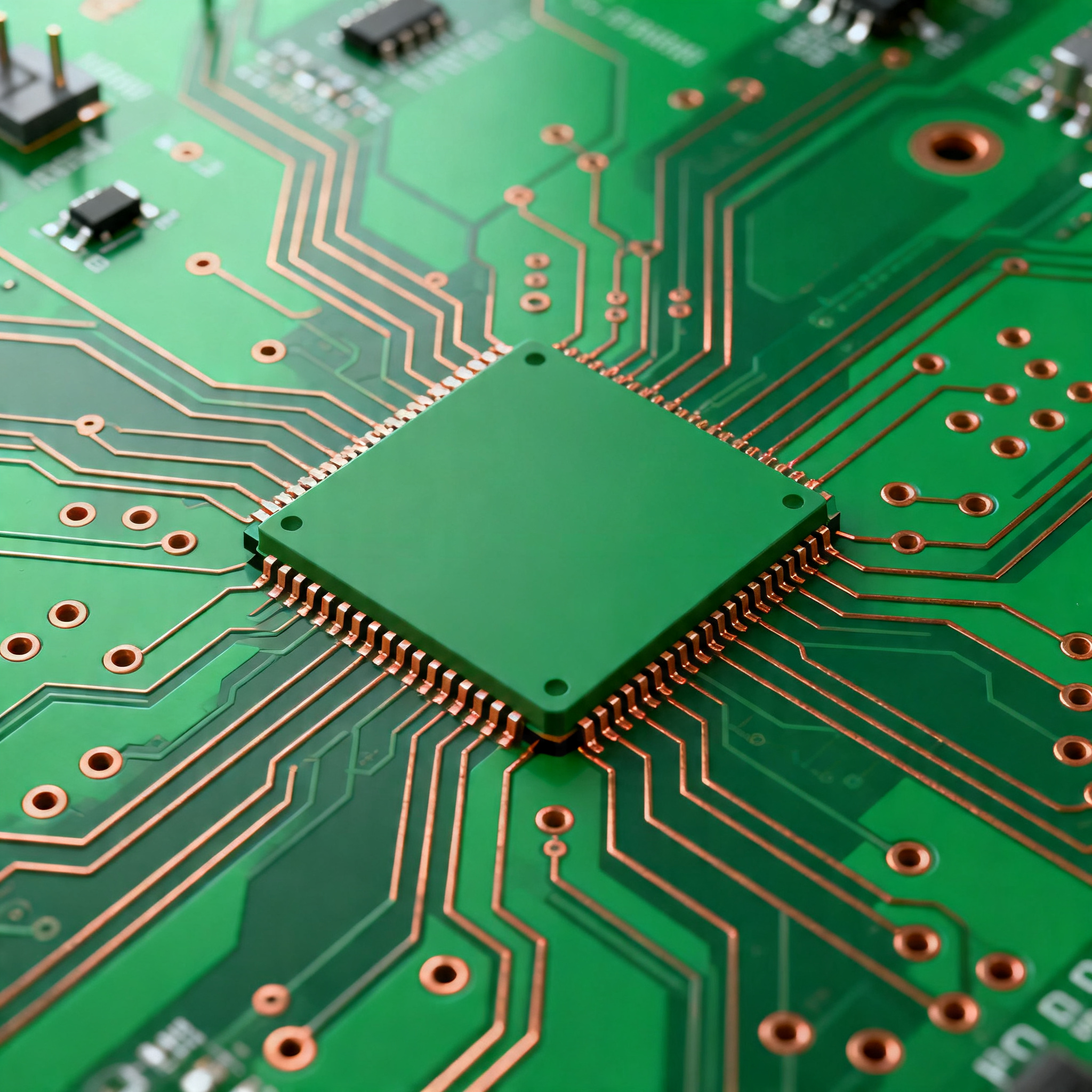
Printed Circuit Boards (PCBs) serve as the backbone of electronic devices, providing mechanical support and electrical connections between components. Key elements of PCB design include layout rules, which define the physical and electrical constraints for trace routing, via placement, and component spacing. Stackup design involves the arrangement of conductive and dielectric layers to optimize electrical performance and manufacturability. Signal integrity is a crucial consideration, ensuring that signals are transmitted without distortion or loss, which is particularly important in high-speed and high-frequency applications. The manufacturing process must also account for material properties, tolerances, and quality standards to ensure reliable and cost-effective production.
Detailed Specifications
In PCB design, understanding and adhering to design rules is crucial for ensuring manufacturability and performance. These specifications dictate the minimum and maximum dimensions for various PCB features, impacting signal integrity and reliability. The following table outlines essential PCB design rules, including trace width, spacing, via sizes, and clearances.
| Design Parameter | Minimum Value | Recommended Value |
|---|---|---|
| Trace Width | 0.15 mm | 0.2 mm |
| Trace Spacing | 0.15 mm | 0.2 mm |
| Via Diameter | 0.3 mm | 0.4 mm |
| Annular Ring | 0.1 mm | 0.15 mm |
| Pad Clearance | 0.2 mm | 0.25 mm |
| Silkscreen Clearance | 0.1 mm | 0.15 mm |
| Solder Mask Clearance | 0.05 mm | 0.1 mm |
| Component Spacing | 0.5 mm | 1.0 mm |
| Aspect Ratio (Via) | 6:1 | 8:1 |
| Drill Tolerance | ±0.1 mm | ±0.05 mm |
| Board Thickness | 0.6 mm | 1.6 mm |
Key Takeaways from the Specifications
The specifications outlined in the design rules table are critical for ensuring your PCB design is manufacturable and meets performance criteria. For instance, trace width and spacing directly impact current carrying capacity and signal integrity. A wider trace can carry more current, but requires more space, affecting the overall layout. Similarly, via sizes and annular ring dimensions are important for maintaining mechanical stability and electrical connectivity. Adhering to these rules helps prevent issues such as short circuits and signal attenuation, which can compromise device functionality.
Layer Stackup Options
Layer stackup is a fundamental aspect of PCB design, influencing signal integrity, thermal management, and overall board performance. Different configurations cater to specific application requirements, balancing factors like impedance control and cost. Below is a table detailing various layer stackup options commonly used in the industry.
| Stackup Type | Layer Count | Applications |
|---|---|---|
| Single Layer | 1 | Simple, low-cost applications |
| Double Layer | 2 | Basic consumer electronics |
| Four Layer | 4 | Improved signal integrity, moderate complexity |
| Six Layer | 6 | Advanced designs with enhanced EMI control |
| Eight Layer | 8 | High-speed, high-frequency applications |
| Ten Layer | 10 | Complex designs, critical impedance control |
| Twelve Layer | 12 | High-density interconnect (HDI) boards |
| Sixteen Layer | 16 | Advanced telecommunications, aerospace |
Practical Implications
Choosing the right layer stackup is crucial for achieving the desired electrical performance and manufacturability. Single and double-layer boards are cost-effective but limited in complexity, making them suitable for simpler applications. As the number of layers increases, so does the ability to manage electromagnetic interference (EMI) and control impedance, which is vital for high-speed and high-frequency designs. However, this also increases manufacturing complexity and cost. Engineers must balance these factors based on application requirements and budget constraints, ensuring the stackup supports the necessary electrical and thermal performance.
Material Properties
The choice of materials in PCB manufacturing significantly affects electrical performance, durability, and cost. Different materials offer varying dielectric constants and loss tangents, impacting signal integrity and thermal characteristics. The following table provides an overview of common PCB materials and their properties.
| Material | Dielectric Constant (Dk) | Loss Tangent (Df) |
|---|---|---|
| FR-4 | 4.2-4.5 | 0.02-0.03 |
| Rogers 4350B | 3.48 | 0.0037 |
| Rogers 4003C | 3.55 | 0.0027 |
| Isola FR408HR | 3.68 | 0.009 |
| Nelco N4000-13 | 3.7 | 0.008 |
| Megtron 6 | 3.4 | 0.002 |
| Arlon 85N | 3.5 | 0.0035 |
| Polyimide | 3.5-4.2 | 0.004-0.009 |
| PTFE (Teflon) | 2.1 | 0.001 |
Application Guidelines
Material selection is a critical step in PCB design, affecting both performance and cost. FR-4 is a versatile and widely used material, offering a good balance of performance and cost for general-purpose applications. For high-frequency applications, materials like Rogers and PTFE are preferred due to their lower dielectric constants and loss tangents, which help minimize signal loss and distortion. Engineers must consider the electrical requirements, environmental conditions, and budget constraints when selecting materials, ensuring the chosen material supports the intended application and lifecycle.
Design Considerations
In PCB design, several factors must be considered to ensure optimal performance and manufacturability. These include trace routing, impedance control, thermal management, and component placement. Proper trace routing is essential for minimizing signal interference and maintaining signal integrity. Impedance control is crucial for high-speed designs, requiring careful consideration of trace geometry and dielectric properties. Thermal management involves designing for efficient heat dissipation, which can be achieved through strategic component placement and the use of thermal vias and heat sinks. Component placement should prioritize electrical performance while considering assembly constraints and mechanical stability. By addressing these considerations, engineers can design PCBs that meet performance specifications and manufacturing requirements.
Step-by-Step Implementation
Implementing a PCB design involves several key steps:
- Define Requirements: Establish the electrical, mechanical, and environmental requirements for the PCB.
- Schematic Design: Create a schematic diagram representing the electrical connections and components.
- Component Selection: Choose components based on performance, availability, and cost considerations.
- PCB Layout: Design the physical layout, including trace routing, via placement, and component positioning.
- Stackup Design: Determine the layer configuration to optimize signal integrity and manufacturability.
- Material Selection: Select materials based on electrical performance, thermal properties, and cost.
- Design Rule Check (DRC): Validate the design against established rules to ensure manufacturability and reliability.
- Prototype and Testing: Fabricate a prototype PCB and conduct testing to verify performance and identify any issues.
Common Issues & Solutions
PCB design and manufacturing can encounter several common issues:
- Signal Integrity Problems: Use proper trace routing, impedance control, and shielding to minimize interference.
- Thermal Management Challenges: Implement thermal vias, heat sinks, and strategic component placement to manage heat.
- Manufacturing Defects: Adhere to design rules and perform thorough design rule checks to prevent defects.
- Component Sourcing Delays: Plan component procurement early and consider alternative suppliers to mitigate delays.
- Cost Overruns: Optimize the design for cost efficiency, balancing performance and material selection.
- EMI Issues: Implement proper grounding and shielding techniques to reduce electromagnetic interference.
Applications & Use Cases
PCBs are used in a wide range of applications, from consumer electronics to industrial systems. In consumer electronics, PCBs are found in smartphones, laptops, and wearable devices, where compact size and high performance are critical. In industrial applications, PCBs are used in automation systems and power electronics, where reliability and thermal management are key considerations. The automotive industry uses PCBs in engine control units and infotainment systems, requiring robust designs to withstand harsh environments. Understanding the specific requirements of each application allows engineers to tailor PCB designs for optimal performance and reliability.
Selection & Sourcing Guide
When selecting and sourcing PCBs, consider factors such as supplier capabilities, lead times, and quality standards. Utilize resources like IC Online to find reliable suppliers and compare options. Ensure suppliers comply with industry standards such as IPC and offer the necessary certifications. Evaluate their manufacturing capabilities, including layer count, material options, and precision tolerances, to ensure they can meet your design specifications and production volumes.
FAQ
- What is the importance of trace width in PCB design? Trace width affects current carrying capacity and signal integrity, with wider traces supporting higher currents.
- How does layer stackup influence PCB performance? Layer stackup impacts signal integrity, EMI control, and thermal management, with more layers offering better performance but higher cost.
- Why is material selection critical in PCB design? Material properties affect electrical performance, thermal characteristics, and cost, influencing overall board performance and reliability.
- What are common challenges in PCB manufacturing? Challenges include maintaining signal integrity, managing thermal performance, and preventing manufacturing defects.
- How can I optimize PCB design for cost efficiency? Balance performance and material selection, adhere to design rules, and consider manufacturing capabilities to optimize cost.
- What role does signal integrity play in PCB design? Signal integrity ensures signals are transmitted without distortion or loss, crucial for high-speed and high-frequency applications.
- How can I ensure reliable component sourcing? Plan procurement early, use multiple suppliers, and verify supplier capabilities and lead times.
- What are the benefits of using advanced materials like Rogers? Advanced materials offer lower dielectric constants and loss tangents, improving performance in high-frequency applications.
- How do I address EMI issues in PCB design? Implement proper grounding, shielding, and trace routing techniques to minimize electromagnetic interference.
- What standards should PCB suppliers adhere to? Suppliers should comply with IPC standards, ensuring quality and reliability in PCB manufacturing and assembly.
Conclusion
The PCB manufacturing industry in 2023 is characterized by advancements in design techniques, material innovations, and manufacturing capabilities. By understanding key trends and adhering to best practices in design rules, stackup configurations, and material selection, engineers can create PCBs that meet the demands of modern electronic applications. Staying informed about industry standards and leveraging reliable suppliers are critical for successful PCB projects, ensuring performance, reliability, and cost-effectiveness in a competitive market.