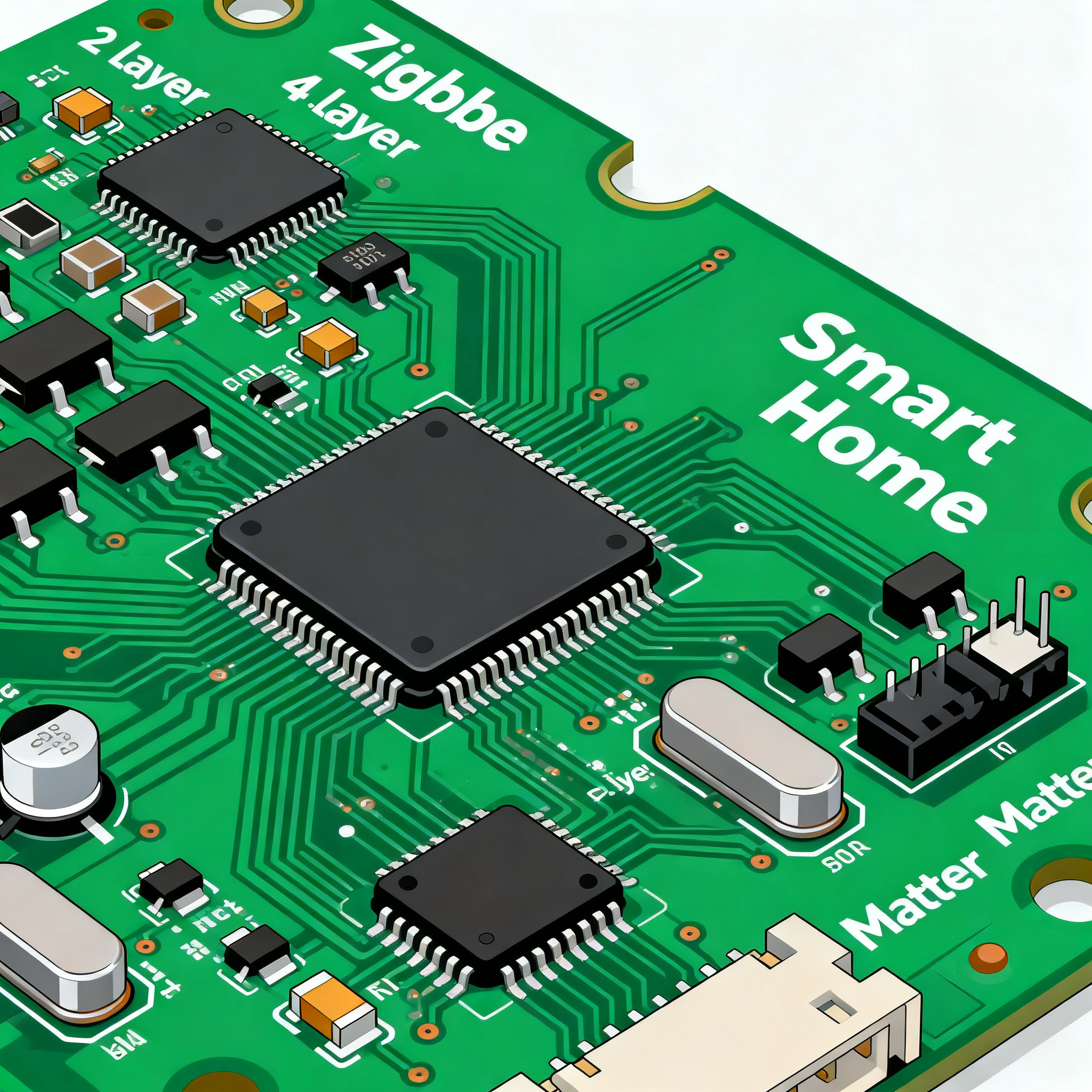
2-Layer to 4-Layer Smart Home PCBA: 3 Real-World Zigbee and Matter Board Builds
From 2-Layer to 4-Layer Smart Home PCBA: 3 Real-World Zigbee and Matter Board Builds Why Smart Home PCB Designers Are Moving from 2-Layer to 4-Layer Stacks Walk through any contract manufacturer’s NPI...
From 2-Layer to 4-Layer Smart Home PCBA: 3 Real-World Zigbee and Matter Board Builds
Why Smart Home PCB Designers Are Moving from 2-Layer to 4-Layer Stacks
Walk through any contract manufacturer’s NPI queue today and you’ll see a quiet but decisive shift: the smart home devices that once shipped on simple 2‑layer FR‑4 are now migrating to 4‑layer stackups. The trigger isn’t a single component change—it’s the convergence of Zigbee 3.0 mesh reliability requirements, Matter’s multi‑protocol interoperability, and the unforgiving physics of 2.4 GHz RF on a cramped board.
In a 2‑layer design, every millimeter of copper does double duty. A trace that carries a sensor interrupt also forms part of the return path for a nearby RF line. The ground “plane” is really a patchwork of pours stitched by vias, and the resulting impedance discontinuities show up as insertion loss and spurious emissions that can kill a product’s wireless range. When you add a PCB antenna, a crystal oscillator, a buck converter, and a handful of GPIOs, the layout becomes a puzzle where signal integrity and EMI control compete for the same thin dielectric.
Four‑layer boards solve this by dedicating entire layers to ground and power. A continuous reference plane directly beneath the RF section gives you a predictable 50 Ω environment, dramatically reducing crosstalk and return loss. For Matter devices that must pass radiated emissions tests without bulky shielding cans, that clean return path often means the difference between first‑pass certification and a costly re‑spin. Even cost‑sensitive products like door sensors and smart plugs are adopting 4‑layer stacks because the BOM savings from eliminating extra filters, ferrite beads, and shielding enclosures can offset the higher bare‑board cost.
The trade‑off is real: a 4‑layer PCB costs more to fabricate and adds a day or two to quickturn lead times. But when you factor in the engineering time spent debugging EMI failures on a 2‑layer board, the equation tilts. Smart home OEMs are learning that a slightly higher PCB unit price is cheap insurance against delayed product launches and field returns caused by flaky wireless connectivity.
How Layer Count Affects RF Performance in Zigbee and Matter Radios
Zigbee and Matter (which runs over Thread or Wi‑Fi) both operate in the 2.4 GHz ISM band. At these frequencies, a PCB trace is no longer a simple wire—it’s a transmission line whose characteristic impedance must be tightly controlled to prevent signal reflections. The difference between a 2‑layer and a 4‑layer board boils down to the quality of the reference plane and the consistency of the dielectric geometry.
In a typical 2‑layer stackup, the RF trace sits on the top layer while the bottom layer serves as a fragmented ground. The distance between the trace and the ground pour is the full board thickness—usually 1.6 mm. To achieve 50 Ω on such a thick substrate, the trace must be impractically wide (often >2 mm), or you must use a coplanar waveguide structure with ground fills on the same layer. Coplanar guides work, but they are sensitive to solder mask thickness, copper etching tolerances, and the exact spacing of the side grounds. The result is an impedance tolerance of ±15% or worse, which leads to measurable insertion loss and degraded antenna matching.
A 4‑layer board places the RF trace on an outer layer with a solid ground plane on the adjacent inner layer (typically layer 2). The dielectric thickness between layers 1 and 2 can be as thin as 0.1 mm to 0.2 mm in a standard 1.6 mm overall thickness stackup. This thin core allows a narrow trace width (around 0.3 mm to 0.5 mm) to hit 50 Ω with a tolerance of ±10% or better, per IPC-2221 guidelines. The continuous plane also provides an uninterrupted return path, minimizing loop area and radiated emissions.
The table below compares key RF parameters for a typical 2‑layer coplanar waveguide design versus a 4‑layer microstrip design, both targeting 2.45 GHz on standard FR‑4.
| Parameter | 2‑Layer (Coplanar Waveguide) | 4‑Layer (Microstrip with Inner Ground) | Notes / Standard |
|---|---|---|---|
| Characteristic Impedance Tolerance | ±15 % (typical) | ±10 % (achievable) | IPC‑2221 design guidance |
| Trace Width for 50 Ω (1.6 mm board) | 0.8–1.2 mm (depending on gap) | 0.3–0.5 mm | FR‑4, εr ≈ 4.5 |
| Insertion Loss @ 2.45 GHz (10 mm trace) | 0.8–1.5 dB | 0.3–0.6 dB | Measured on reference coupons |
| Return Loss (S11) at Antenna Feed | −6 to −10 dB | −12 to −18 dB | Without matching network |
| Crosstalk to Adjacent Digital Line (1 mm spacing) | −15 to −20 dB | −25 to −35 dB | Simulated near‑field coupling |
| Ground Plane Continuity | Fragmented pours, via stitching required | Solid plane on layer 2 | Affects EMI and antenna gain |
| Typical Antenna Gain Variation (PCB antenna) | ±3 dBi across units | ±1.5 dBi | Due to impedance consistency |
These numbers aren’t academic. In a Zigbee door sensor, an extra 1 dB of insertion loss can shrink the reliable mesh range from 15 meters to 10 meters indoors. For a Matter smart plug that must maintain a Thread connection while switching a relay, the cleaner return path on a 4‑layer board prevents the relay transient from coupling into the RF front end—a failure mode we’ve seen repeatedly in 2‑layer prototypes that required last‑minute layout hacks.
Tip: If you must stay with a 2‑layer board, use a thin 0.8 mm substrate instead of 1.6 mm to bring the trace width down and improve impedance control. This approach is common in ultra‑low‑cost sensors but still can’t match the isolation of a dedicated inner ground plane.
2-Layer vs. 4-Layer for Zigbee and Matter: What Three Board Builds Reveal
To ground the theory in real hardware, let’s examine three smart home PCB designs that moved through engineering validation and into production. Each represents a different point on the cost‑performance spectrum, and together they illustrate when a 2‑layer board is still viable and when the 4‑layer upgrade pays for itself.
Build 1: 2‑Layer Zigbee Door Sensor (Contact Sensor)
This is a coin‑cell‑powered magnetic contact sensor using a Silicon Labs EFR32MG22 SoC. The board measures 18 mm × 35 mm and uses a meandered inverted‑F PCB antenna. The stackup is 1.0 mm FR‑4 with a coplanar waveguide feed. The bottom layer is a ground pour stitched with vias every 3 mm. BOM cost is dominated by the SoC and a single CR2032 holder; the bare PCB cost is under $0.30 in 10k volumes. Wireless range in free space reaches 40 meters, but in a typical home with walls, reliable mesh links drop to about 12 meters. The design passed FCC/CE radiated emissions with a small ferrite bead on the battery line. No impedance coupon testing was performed—the PCB shop controlled trace width to ±20 %.
Build 2: 4‑Layer Matter Smart Plug
This design uses a Nordic nRF5340 multiprotocol SoC running Thread and Bluetooth LE for Matter commissioning. The board is 45 mm × 55 mm, 1.6 mm thick, with a 4‑layer stackup: signal‑GND‑PWR‑signal. A chip antenna from Johanson Technology sits in a keep‑out zone with a solid ground reference on layer 2. The inner power plane distributes 3.3 V and 5 V rails. Impedance control is specified at 50 Ω ±10 % with TDR test coupons on every panel. The bare PCB cost is around $1.20 in 10k volumes—roughly 3× the door sensor board, but the BOM saves $0.15 by eliminating a discrete RF matching network and a shielding can over the SoC. Range exceeds 30 meters through two interior walls, and the design passed Matter certification RF tests on the first attempt.
Build 3: 4‑Layer Thread Border Router
This is a mains‑powered hub with Ethernet backhaul, built around a Texas Instruments CC2652P7 and a separate Wi‑Fi module for cloud connectivity. The 6‑layer board (with two additional signal layers) is beyond our scope, but the core RF section is a 4‑layer region with a dedicated RF ground on layer 2 and a power island on layer 3. The PCB antenna is a custom PIFA with a 10 mm × 10 mm keep‑out. The board size is 80 mm × 50 mm. Bare PCB cost is approximately $2.80 in mid‑volume. The design achieves a Thread link budget of 110 dB, enabling whole‑home coverage from a single device. The continuous ground plane was critical for passing EN 55032 Class B radiated emissions without additional shielding.
The table below distills the trade‑offs across these three builds.
| Comparison Metric | 2‑Layer Zigbee Door Sensor | 4‑Layer Matter Smart Plug | 4‑Layer Thread Border Router | Selection Criteria & Failure Boundary |
|---|---|---|---|---|
| Layer Stack | 2‑layer, 1.0 mm FR‑4 | 4‑layer, 1.6 mm (Sig‑GND‑PWR‑Sig) | 4‑layer RF region (Sig‑GND‑PWR‑Sig) | Board thickness driven by mechanical constraints |
| Impedance Control | None (coplanar waveguide, ±20 % trace width) | 50 Ω ±10 %, TDR coupons | 50 Ω ±10 %, TDR coupons | Matter certification expects consistent impedance |
| Bare PCB Cost (10k units) | ~$0.30 | ~$1.20 | ~$2.80 (full 6‑layer board) | Cost delta must be weighed against BOM savings |
| BOM Cost Impact | Includes ferrite bead, extra matching components | No shielding can, minimal RF matching | No external shielding; fewer filter components | 4‑layer can reduce BOM by $0.10–$0.30 |
| Wireless Range (Indoor, 2 walls) | ~12 m | ~30 m | ~35 m (whole‑home) | Range directly affects mesh reliability |
| EMI Certification Outcome | Passed with ferrite bead on DC line | Passed first attempt, no fixes | Passed Class B with margin | 4‑layer reduces risk of radiated emissions failures |
| Design Complexity | High: manual ground stitching, coplanar tuning | Moderate: standard microstrip, clear keep‑outs | Moderate: RF section isolated from digital | 2‑layer demands more RF layout expertise |
| Typical Application | Battery sensors, simple actuators | Mains smart plugs, light bulbs | Hubs, bridges, always‑on controllers | Choose based on power source and range needs |
Notice that the 4‑layer smart plug actually simplified the BOM while improving performance. The border router’s 4‑layer RF section was non‑negotiable: the combination of high‑power Thread radio (+20 dBm) and sensitive Wi‑Fi coexistence demanded the isolation only a continuous ground plane can provide. For the door sensor, 2‑layer remains viable because the tiny board size and low transmit power (+0 dBm) keep EMI manageable, and the cost pressure is extreme.
Design Rules for Smart Home PCBs: Impedance, Ground Planes, and Antenna Keep-Outs
Moving from 2‑layer to 4‑layer isn’t just a stackup change—it’s an opportunity to apply a cleaner set of design rules that directly impact manufacturability and wireless performance. The following guidelines come from dozens of Zigbee and Matter board bring‑ups, and they align with IPC‑2221 for generic design and IPC‑A‑610 Class 2 acceptance criteria for high‑volume consumer electronics.
1. Enforce 50 Ω impedance control from the RF pin to the antenna feed point. On a 4‑layer board with a 0.2 mm prepreg between layers 1 and 2, use a microstrip calculator to determine trace width. Specify the impedance requirement on the fabrication drawing and request TDR test coupons on every panel. This is not optional for Matter devices; the certification test suite includes conducted RF measurements that will expose a mismatched transmission line.
2. Route RF traces on the top layer only. Avoid via transitions on the RF path. If you must change layers, use a ground‑stitched via pair and simulate the discontinuity. Inner‑layer RF routing on a 4‑layer board is possible but requires a symmetrical stripline configuration, which adds complexity and cost. For most smart home products, keep it simple: top‑layer microstrip with a solid ground on layer 2.
3. Create a continuous ground plane on layer 2 under the entire RF section. Do not split this plane for digital or power routing. If the SoC requires multiple voltage rails, use layer 3 as a power plane and connect to the RF section with short, wide traces and local decoupling. A single uninterrupted ground reference is the single biggest factor in reducing spurious emissions and improving antenna efficiency.
4. Respect antenna keep‑out zones. Whether you use a chip antenna, a PCB trace antenna, or an external connector, follow the manufacturer’s recommended keep‑out area on all layers. For a PCB antenna, this means no copper pours, no components, and no mounting holes within the designated area on any layer. On a 4‑layer board, extend the keep‑out to the inner ground plane as specified—typically a clearance of at least 5 mm from the antenna element.
5. Design for high‑volume assembly. Smart home products often ship in the millions. Panelize with breakaway tabs, include fiducials, and avoid placing components within 3 mm of the board edge. Specify IPC‑A‑610 Class 2 workmanship, which balances cost and reliability for consumer environments. A full‑service PCBA partner like Nova PCBA can provide DFM feedback early in the layout phase, catching issues like acid traps, insufficient annular rings, or solder mask slivers that could affect yield.
The table below summarizes key design parameters for smart home PCBs across common protocol requirements.
| Design Parameter | Zigbee 3.0 Sensor (2‑Layer) | Matter over Thread (4‑Layer) | Matter over Wi‑Fi (4‑Layer) | Guidance Source |
|---|---|---|---|---|
| Target Impedance | 50 Ω (coplanar, relaxed) | 50 Ω ±10 % | 50 Ω ±10 % | IPC‑2252, SoC datasheet |
| Min. Ground Plane Clearance under Antenna | 5 mm (bottom layer) | 5 mm (layer 2) | 5 mm (layer 2) | Antenna vendor app note |
| Via Stitching Pitch (ground fence) | ≤ λ/20 (~3 mm) | ≤ λ/20 (~3 mm) along RF edge | ≤ λ/20 (~3 mm) | IPC‑2221, EMI best practice |
| Decoupling Capacitor Placement | Within 2 mm of VDD pin | Within 1 mm of VDD pin | Within 1 mm of VDD pin | SoC hardware design guide |
| Trace Width for 50 Ω (εr=4.5, 1.6 mm board) | 0.8 mm (with 0.2 mm gap) | 0.35 mm (layer 1‑2 prepreg 0.2 mm) | 0.35 mm | Calculated; confirm with fab |
| Minimum Annular Ring (Class 2) | 0.05 mm (external) | 0.05 mm (external) | 0.05 mm (external) | IPC‑A‑610 Class 2 |
| Panelization Method | V‑score or tab‑routing | Tab‑routing with mouse bites | Tab‑routing | Assembly partner recommendation |
One common pitfall we see is designers treating the 4‑layer stackup as a license to ignore layout discipline. A solid ground plane helps, but it won’t save you if you route a noisy switching node directly under the antenna feed or place a crystal oscillator on the opposite side of the board without local shielding. Always review the RF section in isolation, and simulate or measure the antenna impedance with a vector network analyzer before freezing the design.
Smart Home PCB Assembly FAQ: What Engineers and Buyers Ask About Layer Transitions
Q: What is the typical cost increase per board when moving from a 2‑layer to a 4‑layer PCB for a Zigbee sensor?
A: Depending on volume and board size, expect a 20–40 % increase in bare PCB cost. For a small sensor board, that might mean going from $0.25 to $0.35 at 10k units. However, the improved yield and reduced EMI re‑spins often offset this in production. When you factor in BOM savings from removing extra filters and shielding, the total cost of ownership can actually favor the 4‑layer design.
Q: Can I still use a 2‑layer PCB for a Matter over Thread device?
A: Yes, if the board is small and you can maintain a solid ground plane on one side with careful routing. A 0.8 mm thick 2‑layer board with a coplanar waveguide can work for low‑power devices. But 4‑layer is recommended for consistent antenna performance and certification ease. Matter’s multi‑vendor interoperability testing is unforgiving; a marginal RF design that works with one border router may fail with another.
Q: How does layer count affect lead times for prototype assembly?
A: 4‑layer PCBs typically add 1–2 days to standard quickturn fabrication. A 2‑layer prototype might ship in 3–4 days, while a 4‑layer board takes 5–6 days. Partnering with a full‑service PCBA provider like Nova PCBA can streamline the entire process—they manage both bare‑board fabrication and assembly under one roof, often reducing total turnaround time by a day or more compared to splitting the supply chain.
Q: What IPC standards should I reference for impedance control on smart home boards?
A: IPC‑2221 for generic design rules, IPC‑A‑610 for assembly acceptance criteria, and IPC‑2252 for controlled impedance design guidance. For RF‑specific stackup recommendations, also consult your SoC vendor’s hardware design guide—Nordic, Silicon Labs, and TI all publish detailed reference layouts that align with these IPC standards.
Q: Do 4‑layer boards require different testing for Zigbee/Matter certification?
A: No, the certification test plans are the same regardless of layer count. However, a cleaner layout reduces the likelihood of failing radiated emissions or receiver sensitivity tests, saving time and cost. We’ve seen 2‑layer designs require multiple lab visits to debug EMI issues, while equivalent 4‑layer boards pass on the first attempt.
Q: When does it make sense to move from 2‑layer to 4‑layer for a cost‑sensitive product?
A: When board size constraints force tight routing, or when you need to pass regulatory EMI tests without additional shielding. The BOM savings from removing extra filters, ferrite beads, and shielding cans can justify the layer upgrade. A good rule of thumb: if your 2‑layer layout requires more than two ferrite beads or a shielding can over the RF section, you’re probably better off moving to 4‑layer and simplifying the BOM.
The decision to move from 2‑layer to 4‑layer is rarely about the PCB cost alone. It’s about the total cost of engineering time, certification risk, and field reliability. For smart home products that live or die by wireless connectivity, a 4‑layer stackup is increasingly the default choice—and the three builds we’ve examined show that even cost‑sensitive designs can benefit from the cleaner RF environment it provides. Whether you’re prototyping a new Zigbee sensor or scaling a Matter smart plug to high volume, engaging an experienced PCBA partner like Nova PCBA early can help you navigate the stackup decision, impedance control requirements, and DFM rules that turn a good design into a great product.
References & Further Reading
- IPC — Association Connecting Electronics Industries (IPC‑2221, IPC‑A‑610, IPC‑2252)
- Nova PCBA — Professional PCB Assembly Services
- Connectivity Standards Alliance (CSA) — Matter Specification
- Zigbee Alliance — Zigbee 3.0 Protocol
- Nordic Semiconductor nRF5340 — Multiprotocol SoC for Matter/Thread
- Silicon Labs EFR32MG22 — Zigbee SoC
- Texas Instruments CC2652P7 — Thread/Zigbee Wireless MCU
- Johanson Technology — Chip Antennas and RF Components